Compact & efficient dual output DC source
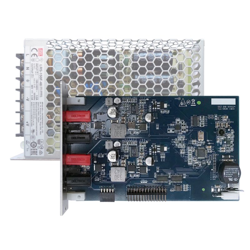
DCM224 POWER MODULE
- Up to 3 modules per BB3 for a total power of up to 465 W and six outputs individually controlled or combined (tracking mode)
- 1 – 24 V, set and readout resolution 10 mV
- 100 mA – 4.9 A, set resolution 10 mA, readout resolution 20 mA, ±6%
- Isolated (“floated”) output
- PWM LED dimming
- MCU controlled switching frequency with dithering
- On-board STM32F373C8T6 32-bit ARM Cortex®-M4 MCU, 64 KiB Flash, 32 KiB SRAM, LQFP-48 package
- Power input: 48 Vdc (e.g. Mean Well LRS-150F-48)
- Combined max. output power: up to 155 W
- Separate control of each power outputs
- Voltage regulation (CV), 1 – 24 V. Voltage set resolution (U_SET): 12-bit, read resolution (U_MON): 15-bit
- Current regulation (CC), 100 mA to 4.9 A. Current set resolution (I_SET): 12-bit, read resolution (I_MON): 15-bit
- PWM LED dimming
- MCU generated two counterphase switching frequencies
- On-board power pre-regulator and bias power supply
- Output Enable (OE) and Constant Current mode (CC) LED indications
- Output LC filter for improved ripple and noise
- On-board 4 mm power output terminals with standard (19.05 mm) pitch
- Pass-thru connector for Vout- coupling with other DIB power modules
- Galvanically isolated SPI bus for communication with MCU board
- I2C EEPROM for storing board specific configuration and calibration parameters
- Dimensions: 155 x 95 mm, 4-layer PCB
|
Current version |
r3B3 |
|
Status |
Active |
|
BOM |
Yes (TME, Mouser, Digikey, Farnell, RS) |
|
File repository |
https://github.com/eez-open/dib-dcm224 |
|
License |
|
|
Contributions |
|
Output power terminals |
Series |
Parallel |
Split rails |
Common ground |
|
No |
No |
No |
Yes |
Block diagram
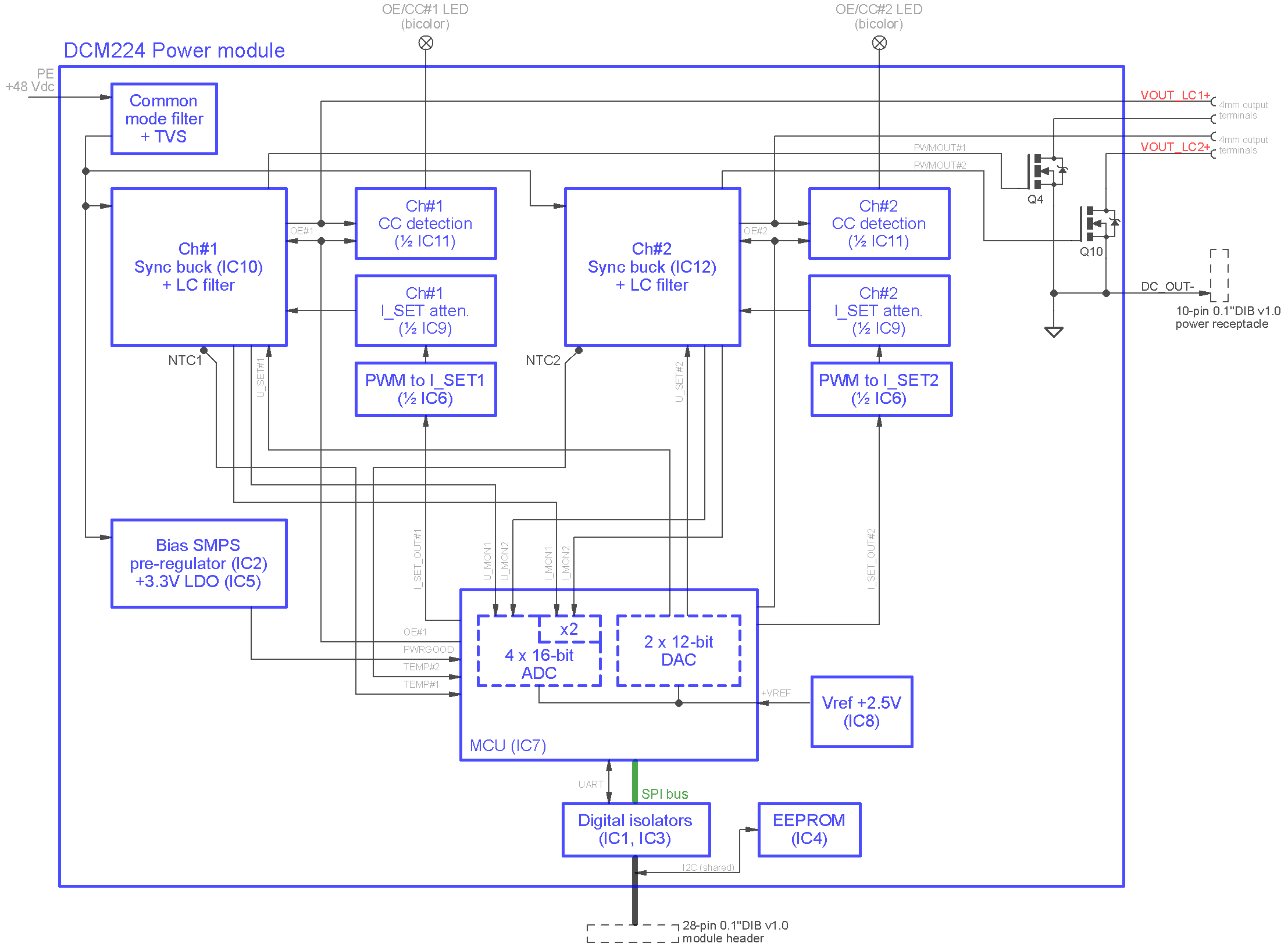
Fig. 1: DCM224 power module block diagram
Bias power supply
The bias power supply is built around low power buck step-down converter (IC2), and thanks to coupled inductor (TR1) it provides both positive and negative rails of about 8 V for analog section. Digital section is powered with +3.3 V that is derived from LDO (IC5).
The IC2 also provides POWERGOOD signal that indicates MCU what is module’s power condition. It is related to UVLO (under-voltage lockout) functionality that is controlled with voltage divider consists of R3, R6. Therefore the step-down converter will cut-off power when input voltage drops below +26.4 V, and starts again when it rises above +27.3 V.
EEZ DIB interface
The DCM224 module interface with the MCU module is accomplished over the 28-pin 0.1” right angled header (X2). Since its power output has to be isolated (“floated”) all digital control lines has to be isolated. Therefore two high speed digital isolators (IC1, IC3) are used.
Onboard I2C EEPROM (IC5) provides storage for module-specific information such as its ID, calibration data, working hours counters, etc. Please note that it is on the A-side of the isolation barrier, because the same I2C bus is shared among all modules (that includes AUX PS module, too). It address is defined by R12, R13 and R14 pull-up resistors and ground connections on the backplane.
The MCU (IC7) on Fig. 5. is a SPI “slave” that communicates with the “master” MCU on the MCU module.
Power channel outputs can be synchronized with power outputs on the other modules thanks to OE_SYNC signal that is also controller by “master” MCU.
Fig. 2: Bias power supply, DIB interface
Digital control
The DCM224 comes with STM32F373C8T6 (IC7), a mainstream mixed signals MCUs ARM Cortex-M4 core with DSP and FPU with 64 KiB Flash, 72 MHz CPU and MPU. It’s also featuring 12-bit DACs and 16-bit Sigma-delta ADCs (with inputs multiplexer).
Controlling DCM224 power channels require two DAC channels (one for programming voltage and current) that gives four channels in total. Since selected MCU comes only with three DAC outputs, two are used for set output voltage (U_SET_OUT#1, U_SET_OUT#2) and remaining two required to set output currents are generated using MCU’s PWM outputs.
16-bit ADCs are used for monitoring output voltage and current. Power output voltage value is derived with simple voltage dividers (R38, R45 on Fig. 4., and R61, R68 on Fig. 5.) that are set to provide +2.5 V for full scale. ADC voltage reference (+VREF) is provided by IC8.
Power output current value is measured by DC/DC controller (IC10, IC12) and available on its ISMON pin. Since its output range is from zero to just 1.5 V, a gain of x2 is selected in firmware on ADC’s current inputs (I_MON#1, I_MON#2).
Output voltage programming
The output voltage is programmed by affecting FB pin voltage that is set by voltage divider R37, R44 on channel 1 and R60, R67 on channel 2 (the DAC outputs are brought via R46 and R69).
Output current programming
Conversion of PWM to analog signals for current programming is accomplished with DC filtering and additional ripple cancellation (IC6). The output current programming value comes to CTRL1 input of the DC/DC controller and it has to be in range from 0 to +1.5 V. Therefore an op-amp (IC9B, IC9A) is used to attenuate current programming signal by 0.45 since its range is from 0 to +3.3 V.

Fig. 3: Digital control and temperature sensors
Temperature is measured by two NTCs (NTC1, NTC2) that make voltage dividers with R21 and R22. NTC’s are positioned close to DC-DC controllers (IC10, IC12). Voltage dividers outputs vary with temperature and they are brought to ADC inputs TEMP#1 and TEMP#2.
The MCU firmware could be uploaded by set BOOT0 input to +3.3 V during the power-up or reset and use UART for communication with programmer (that could be “master” MCU on the MCU module). Additionally, for development purposes it is possible to solder X3 connector and used ST-LINK compatible in-circuit debugger/programmer.
UART communication that is required for firmware upload needs accurate clock and that is a main reason why external clock source (Y1) is used instead of internal RC 8 MHz oscillator.
Power channels
The DCM224 module comes with two identical power channels based on 60 V high current step-down synchronous LED driver controller (IC10, IC12) as shown on Fig. 4 and Fig. 5. They are sharing the same power input of +48 Vdc and consequently share the same ground.
The LT3763 comes current programming and monitoring that can be used for digital control and can work in CV (Constant Voltage) or CC (Constant Current) mode.
Unfortunately, it does not provides an indication of the mode of operation. Therefore the CC mode indication is accomplished on presumption that it currently does not works in CV mode and that is when voltage on the FB pin is below 1.4 V. Comparators (IC11B, IC11A) are used to check voltage level on the FB1 and FB2 pins that are buffered with IC11C, IC11D to minimize interference with the CV control loop.
Comparator’s outputs are brought to MCU’s digital inputs CC#1, CC#2 that can be used by firmware to indicate that on the TFT display or by activating red LEDs of bicolor LED1, LED2 (via Q5, Q11). Activation of that LEDs depend also of channel output state, and its disabled by when channel’s output is disabled.
Power outputs state are directly controlled by MCU digital outputs OE#1, OE#2 brought to DC/DC controller’s EV/ULVO input and that signals are used to drive green LEDs of bicolor LED1, LED2 (Q6, Q12).
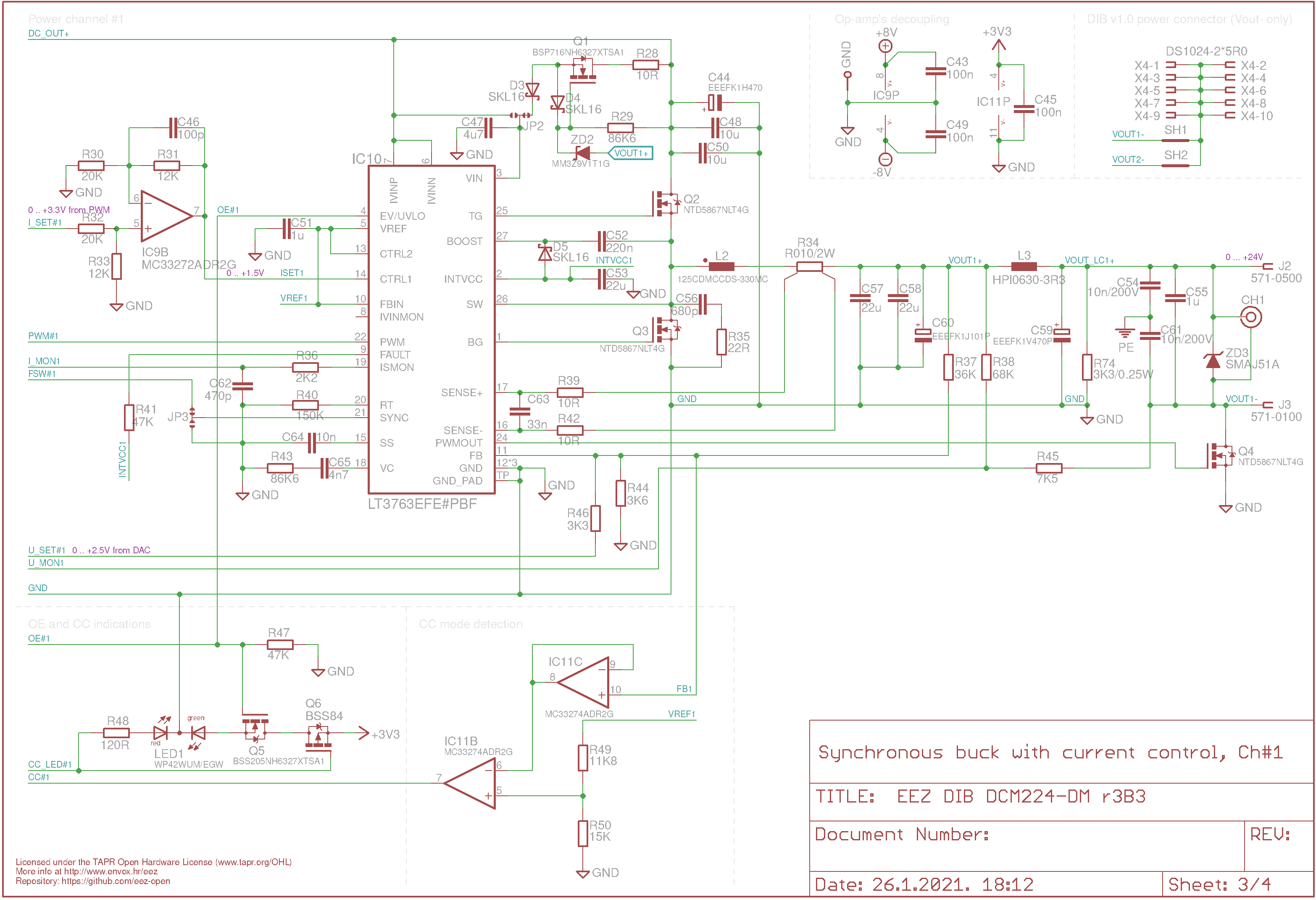
Fig. 4: Sync buck for power channel #1
The DC/DC converter is equipped with internal regulator with Vin as a power input and provides +5 V on its output that is used for powering internal logic and to some extent external circuit if total consumption does not exceeds 60 mA. Measured internal consumption is about 22 mA that with voltage drop of 43 V requires that almost 1 W is dissipated. Thermal stress is reduced by adding simple voltage regulator (Q1, Q7) on the Vin pin. It is tracking power output voltage and insure difference of at least +7 V (defined by ZD2, ZD4 and Vgs(th) that is 1.8 V max. for the selected MOSFET) that is required for normal operation. Therefore the internal regulator will be supplied with about +7 to 31 V instead of continuous +48 V that reduces its dissipation significantly, or better to say, move it to the voltage regulator’s MOSFET that comes in bigger package and can be cooled down much easier.
When DC/DC converter is disabled, voltage on the Vin rises to the power input value (+48 V). To avoid damage of the MOSFET (Q1, Q7) in that case, diodes D3, D4 and D6, D7 as protection are added.
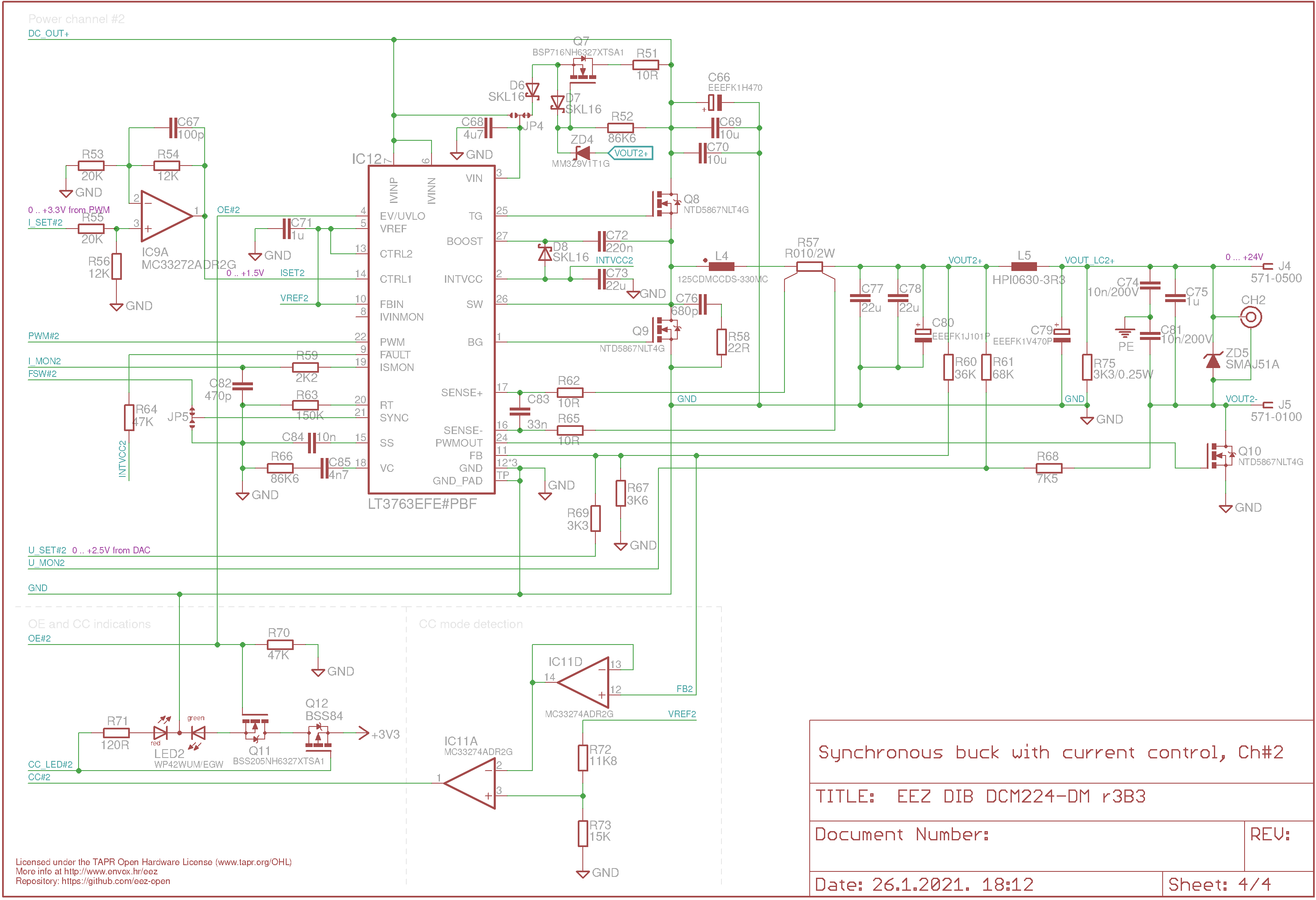
Fig. 5: Sync buck for power channel #2
Power outputs are equipped with LC filters (L3, C59 and L5, C79) to reduce ripple and noise and protected against over-voltage and reverse polarity with TVS diodes ZD3, ZD5.
PCB layout
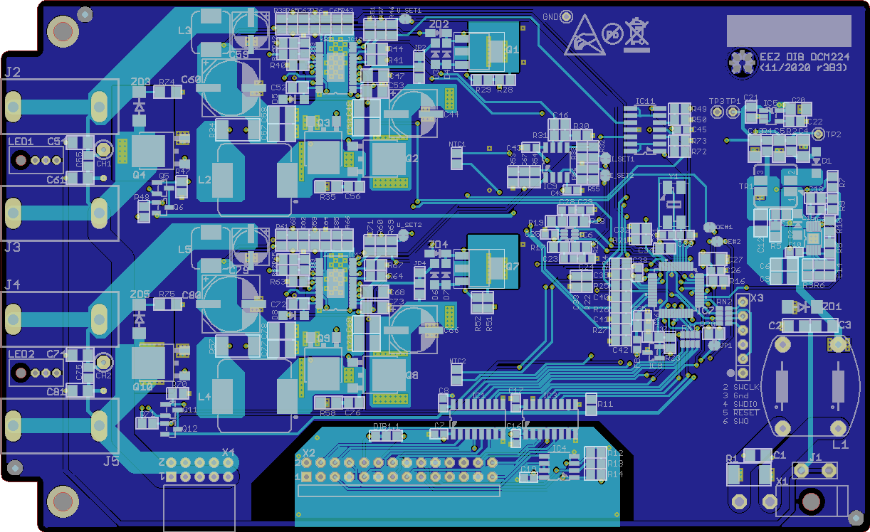
Fig. 6: PCB Top (cyan) and bottom (blue) layer
DCM224 is an open hardware design: schematics, PCB layout, Gerber files and BOM are available on GitHub.
Firmware images
Module firmware download procedures are described in BB3 User manual, Chapter 13.3.
|
Project |
Type |
Source |
Firmware image (download .hex or .dfu file) |
|
|
Module |
 |
|||
|
Module |
 |
|||
Downloads
PCB color: Blue, CE: Yes
Status: Active
PCB color: Green, CE: No
Status: Retired (GitHub archive)
Join our community
You can meet us at Discord where there is an ongoing discussion with other members and supporters about usage, improvements, issues, etc.
Open Source
Schematics, BOMs, mechanical details, code, manuals are on GitHub and are available for servicing, modification and improvement, learning, etc.