CF-DIC with HV buck
The power output section of the EEZ AC/DC converter is using the topology called current-fed dual inductor converter (CF-DIC), that evolved from Single Inductor Converter (or SIC) presented for the first time in the article Filho, Barbi (1996), A comparison between two current-fed push-pull DC-DC converters-analysis, design and experimentation.
Basic components for converter’s topologies with single (SIC) or dual inductor (DIC) are shown in Fig. 1 and Fig. 2.
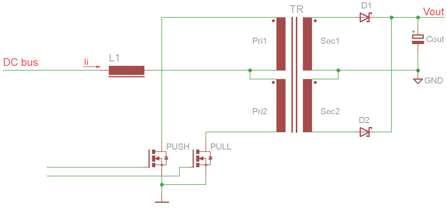
Fig. 1: Single Inductor Converter (SIC)
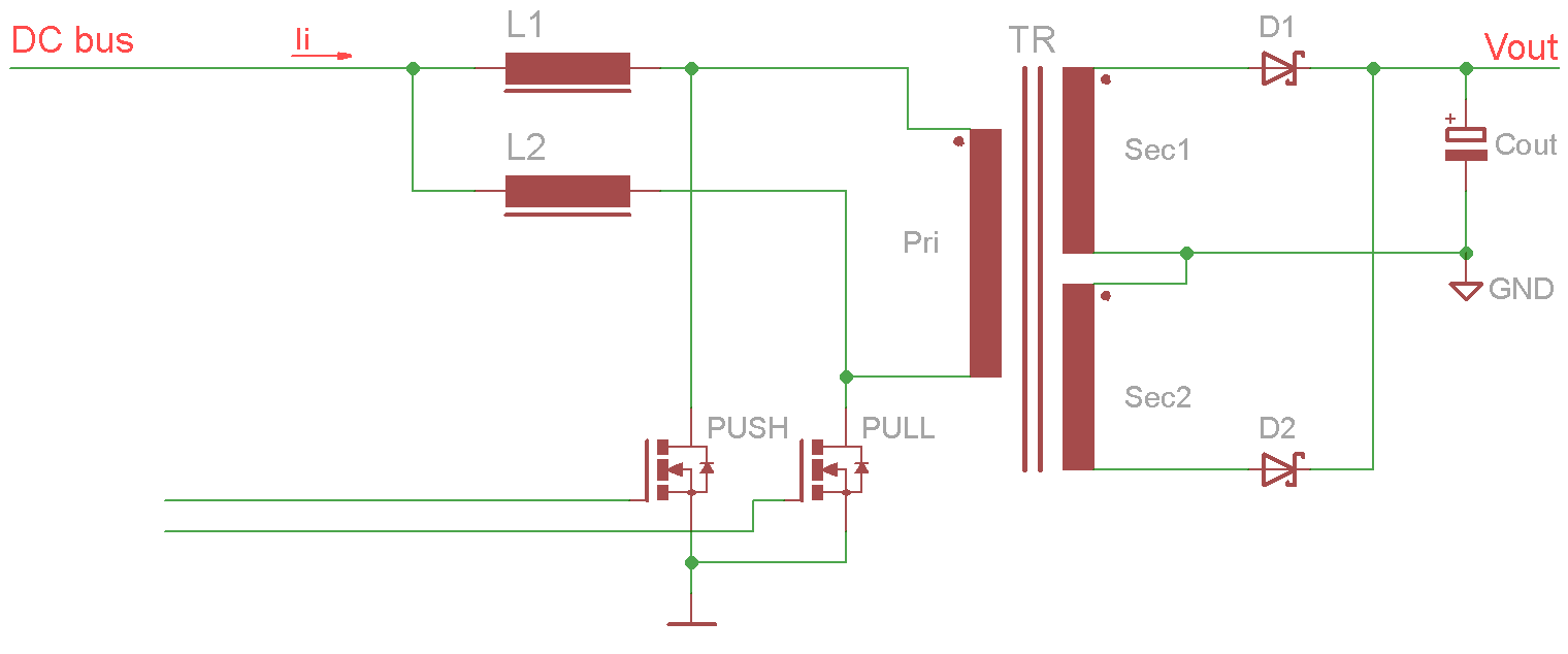
Fig. 2: Dual Inductor Converter (DIC)
A list of DIC benefits over SIC topology is presented in the above mentioned article that can be summarized as the following list of advantages:
- Voltage across the switch is 50% lower, hence switching components stress is lower
- Transformer require only one primary coil and peak volt-ampere is 50% lower
- Input inductor current is 50% lower (a cheaper/smaller inductor can be used)
- Smaller current ripple and rms current in the output capacitor
- Slightly smaller switches rms current
- Inductor switching frequency is 50% lower (hence smaller losses)
The final topology is shown on Fig. 3. A HV (high voltage) buck section has been added at the input that can be used to change duty cycle while DIC’s push-pull (PP) section is working with fixed duty cycle. In a way PP section serve as a “DC transformer” (mind quotation marks here) that isolate primary from secondary side of the HV buck.
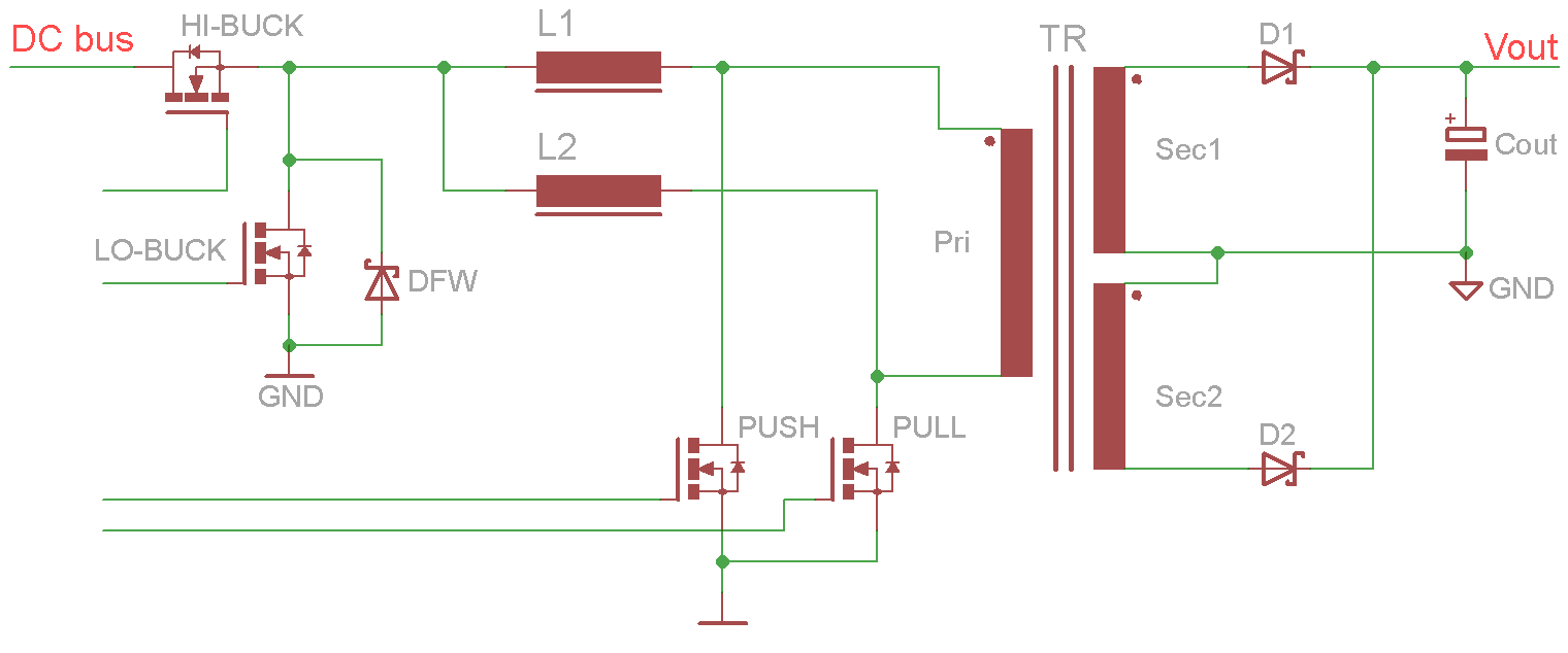
Fig. 3: DIC with HV buck
Driver circuits for both buck (synchronous) and PP sections can be found in TI’s LM5041B PWM cascaded controller. It include outputs that can be used to drive PP section directly but with fixed duty cycle that is set to 50%. Depends of chosen topology, i.e. voltage-fed or current-fed its PUSH and PULL outputs can be programmed with dead-time or overlap-time respectively.
Driver signals overlapping is of paramount importance since neither of DIC inductors should be disconnected at anytime. That will induce a huge voltage that will instantly destroy one of the switching elements (MOSFETs in our case).
PP switching frequency is derived from HV buck section frequency that is twice as much higher and set with external resistor.
How it works
The following steps is an overview of important facts during operation:
- Vin is switched on (first half cycle). HI-BUCK MOSFET and one of the PP MOSFETs (e.g. PUSH) are turned on. The L1 inductor between them is connected to the full voltage (almost Vin) and current in it is rising following the dI = U / L x dt
- When PWM time is expired, HI-BUCK is turned off and L1 inductor is trying to keep its current (Iend) to flow in the same direction. That current flow is preserved thanks to LO-BUCK MOSFET that is turned on (when expire dead-time after HI-BUCK is turned off). The PUSH MOSFET is still conducting. At the L1 inductor ends we have almost short-circuit condition (i.e. the major voltage drop is caused only by Rds, on of LO-BUCK and PUSH MOSFET). Following the same law of dI = U / L x dt current change will be minor since voltage is small (about 1 V) hence we can consider that current is constant (e.g. Iend is still unchanged).
- Just prior then PUSH MOSFET is switched off, PULL MOSFET is switched on (as defined with overlap time) and connect its end of primary coil to the ground. Otherwise when PUSH MOSFET is turned off both primary coil’s ends will be left unconnected and the voltage on both drains will go into infinity (with disastrous outcome for one or more components!). PULL MOSFET also connect its inductor (L2) to the ground and new HV buck cycle is starting that is now charging L2 inductor.
- Short overlap time is expired and PUSH MOSFET is turned off and voltage on its drain reach primary coil’s Vclamp value (since its other end is grounded). Other end of the primary coil, that is connected to the switched off PUSH MOSFET is now behave as an accumulator that is charging and has Vclamp potential. Current thru L1 has Iend value and is now flowing thru the primary coil.
- L1 inductor potential is now Vin - Vclamp, because HV buck hi-side period is active. Since it was previously shorted and preserve Iend current, that current is now decrease slowly since a small voltage difference exists between its ends.
- HI-BUCK is turned off again, and its voltage drops to LO-BUCK voltage drop (e.g. -Vd). L1 inductor has now Vclamp - (-Vd). The voltage difference is now much higher and current thru L1 inductor is falling much faster supplying the primary coil. L2 inductor has a constant current and its captured by short-circuit caused by PULL MOSFET conduction state and waiting that PULL MOSFET be turned off that it can start to flow into primary coil that will be reversely polarized in that moment.
- Prior then PULL MOSFET is switched off (during the overlap period) now the PUSH MOSFET is turned on and “catch” its side of the primary coil, PULL MOSFET is turned off and current is continue to flow in other end of the primary coil that is reversely polarized
- … and the whole cycle is repeated over and over again.
The CF-DIC (current feed DIC) with short overlap time can be interpret as two boost converters that works in counter-phase with duty cycle a slightly over 50% and which load behind rectifiers is Vclamp. That means that the almost same rule is applicable for DIC inductor’s calculation, where their supply is the HV buck and average voltage of it pulses can be used as a DC source.
Output Vclamp on the Cout is reflected/mirrored on the primary coil proportionally to the transformer transfer ratio (Np/Ns). For example if Vclamp (i.e. converter’s output voltage) is set to 10 V with transformer ratio N = 2 we’ll get 20 V on the primary coil ends despite the fact that DC bus voltage is 325 Vdc (rectified 230 Vac).
Vclamp that is reflected/mirrored on the primary side can be seen as a voltage source with certain internal resistance. Therefore primary coil behaves as voltage source what is result of such heavy capacitance load. That load is necessary since it directly define its Vclamp.
Finally, it is worth mentioning that CF-DIC topology is suitable for providing high voltage outputs and if designed with fixed outputs it can easily provide multiple outputs similar to flyback but with output power that easily reach few kilowatts with much lower stress on the output capacitors (that means their prolonged lifetime) and better filtration then flyback.
Despite the fact that CF-DIC belongs to the group of so-called hard-switched topologies, when properly built, it can provide almost textbook-like wave shapes that results in reduced EMI that is comparable with resonant topologies.
Primary side
Schematic diagram of the CF-DIC primary side is shown on Fig. 4. that contains Cascaded PWM controller, isolated driver with HV buck, CF-DIC with diode clamping and protection circuits.
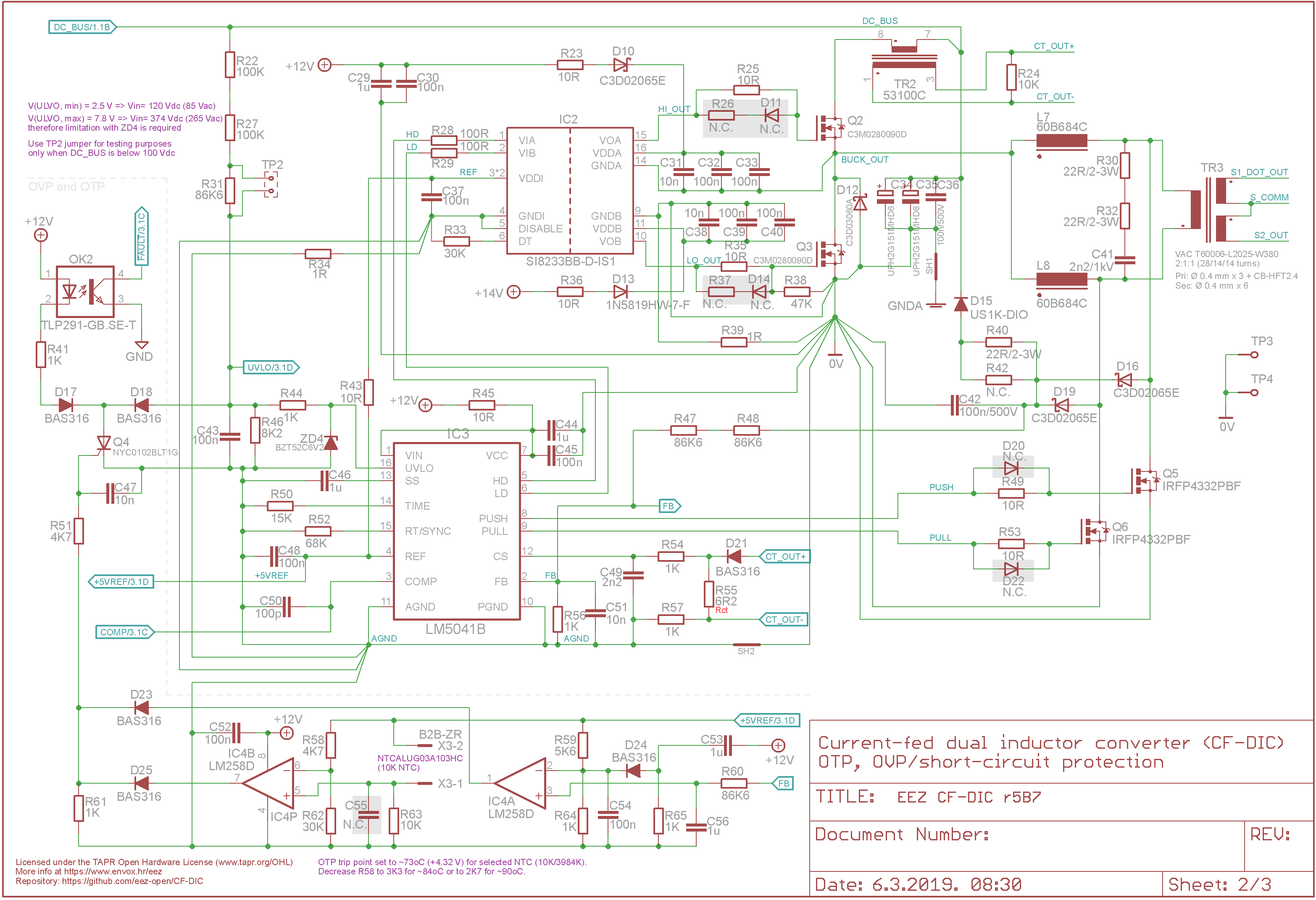
Fig. 4: CF-DIC, HV buck and protection circuit
HV buck
The HV buck is of synchronous type, i.e. it incorporate a lo-side switch. A high-performance SiC 900 V C3M0280090D switches are used (Q2, Q3) for increased efficiency thanks to its speed that is in order of magnitude higher then ordinary Si MOSFETs, fast intrinsic diode with low reverse recovery (Qrr) and regardless of its relatively high Rds, on value (280 mΩ). D12 is not mistakenly connected in parallel with lo-side MOSFET. Since SiC type is used its performance in third quadrant is not so good in comparison with ordinary (Si) MOSFET. Therefore D12 is assisting it for a short time. That issue could be resolved if its driver is capable to deliver negative (-3 to -4 V) Gate voltage when it is turned off, what is not the case. The Q2 and Q3 comes in TO-247 package to insure good creepage distance without need to introduce additional precautionary measures such as PCB milling between terminals or applying varnish over exposed PCB pads.
The LM5041B buck output stage is not capable of directly driving buck MOSFETs. Therefore a Hi-side/Lo-side MOSFET driver (IC2) is required. A Si8233 dual driver is chosen that is capable to withstand up to 1.5 kVrms peak driver-to-driver differential voltage and can deliver up to 4 A. In addition it provide isolation between signal and power ground that can greatly improve EM immunity of the A-side (where is signal ground) and simplify PCB layout design. A drawback of deployment of isolated driver is that each of its side require separate power supply, and A-side max. supply voltage is just 5.5 V. Therefore for powering it a separate 5 V power source should be provided. Fortunately, A-side power consumption is very low (typ. 2 mA, max. 3 mA) and LM5041B REF output that is stable voltage reference is used which can deliver no less then 15 mA (typ. 20 mA). The Si8233 also offer adjustment of dead-time (DT input pin).
Powering hi-side N-ch MOSFET require bootstrap power that is provided from AUX output that is also used for powering the LM5041B (but separately from VIPer35 as already mentioned above). As the bootstrap diode (D10) a high performance SiC diode is used that has extremely low reverse recovery as its SiC MOSFET counterpart that can decrease level of stress to the AUX power supply significantly. On the other side (lo-side) D13 is included to provide better “symmetry” with hi-side supply voltage.
The HV buck output HD and LD switching frequency is defined with RT (R52) connected to the RT/SYNC LM5041B input. This input is highly sensitive and RT has to be placed as close as possible to the LM5041B with good connection to AGND (signal ground). The RT value can be calculated from:
RT = (1/Fsw - 235 x 10-9) / 182 x 10-12
For example, for Fsw = 66 kHz, RT value is about 82 kΩ that is initially used for testing and is changed to 68 kΩ and give us in return Fsw of about 80 kHz.
For normal operation of the HV buck stage a current measure is also required. That is achieved by inserting 1:100 current transformer (TR2) on the DCbus line between Cbulk (C34, C35) and HV buck input (hi-side MOSFET). TR2 is rated for 500 Vdc that should provide enough safety margin for the continuous work. If better margin is needed few other model exists in the same form factor that provide up to 1 kV of isolation between primary and secondary (e.g. EPCOS B82801B series).
The LM5041B’s PWM comparator compares the current sense (CS input) signal to the voltage at the COMP pin. The output stage of the internal error amplifier generally drives the COMP pin. At duty cycles greater than 50%, current mode control circuits are subject to sub-harmonic oscillation. By adding an additional fixed ramp signal (slope compensation) to the current sense ramp, oscillations can be avoided. The LM5041B integrates this slope compensation by buffering the internal oscillator ramp and summing a current ramp generated by the oscillator internally with the current sense signal.
The LM5041B also provides cycle-by-cycle OCP (over-current protection) that is using current transformer output. If the voltage at the CS comparator (CS pin voltage plus slope comp voltage) exceeds 0.5 V the present buck stage duty cycle is terminated (i.e. cycle by cycle current limit). The CS input pin voltage is defined with TR2 ratio (1:100) and termination resistor R55. Voltage on R55 should be still below 0.5 V threshold for lowest Vin and max. allowed Iout. Fig. 5 shows voltage on the CS input for selected value of 6.2 Ω for Vin=115 Vac and Iout=5.4 A.
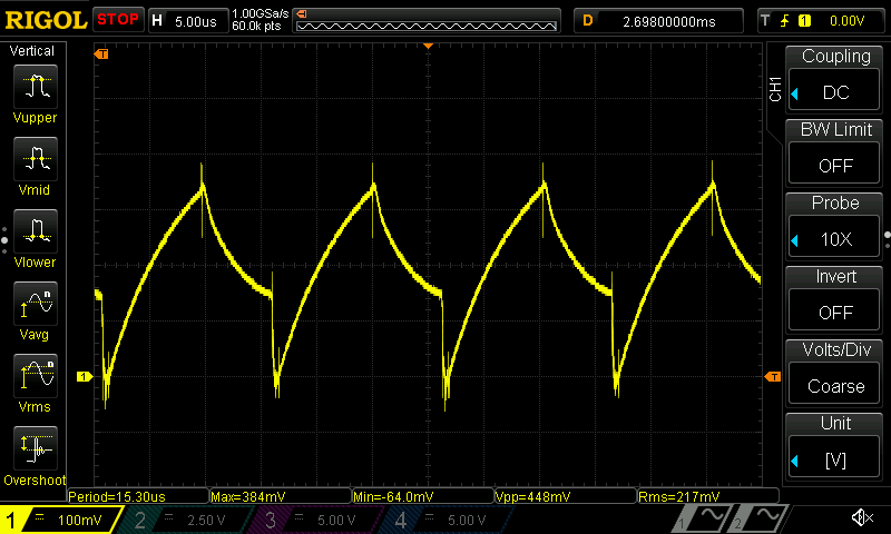
Fig. 5: CS voltage for Vin=115 Vac and Iout=5.4 A
Measured value of the 448 mV is still within 0.5 V range therefore, no cycle-by-cycle current limitation can be expected. Of course, for the Vin=230 Vac, the CS input voltage is predictably even lower as shown on Fig. 6.
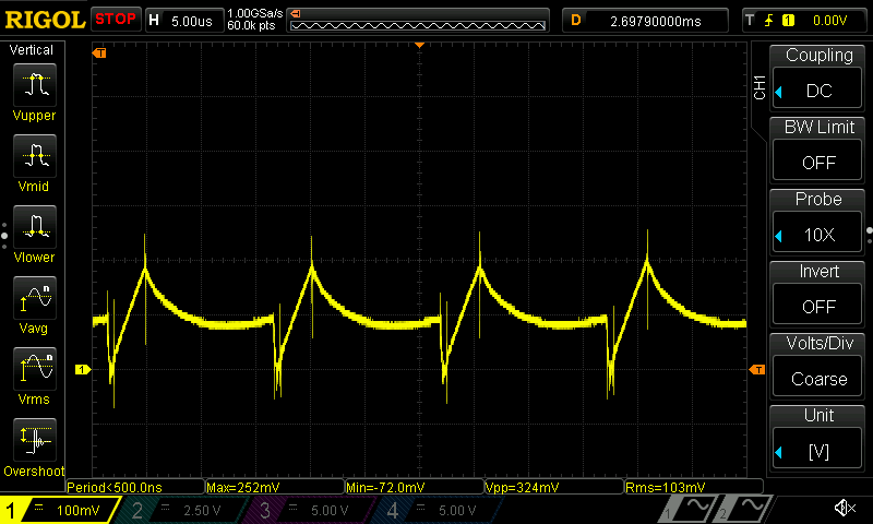
Fig. 6: CS voltage for Vin=230 Vac and Iout=5.4 A
The buck outputs (HD, LD pins) state is dependent of the UVLO input that is used to define min. Vin threshold set with voltage divider consist of R22+R27+R31 and R46. Set threshold (with small hysteresis) is internally set to 2.5 V that means that HV buck will be stopped if Vin goes below 90 Vdc (for R46=8.2 kΩ). That sounds quite low since it equals to only 66.5 Vac, rms. But, we have to take into account input ripple on the Cbulk that increases as load is increased. Its value is far from negligible and for max. power output it reach about 60 Vpp as shown on Fig. 7. With Vin, min=94 V it’s just about the fringe of the working range, what is still fine since Iout is about 10% over the desired Imax.
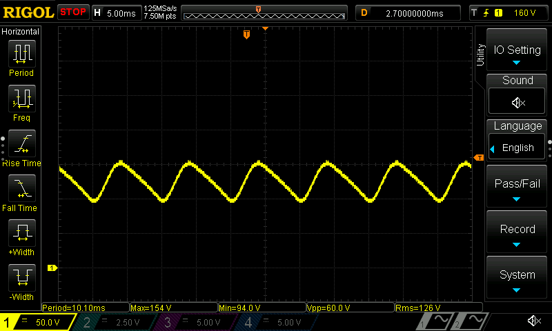
Fig. 7: Cbulk ripple for Vin=115 Vac and Iout=5.4 A
Measured on the UVLO pin directly, above shown ripple will be seen as shown on the Fig. 8.
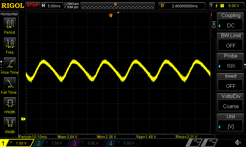
Fig. : UVLO input for Vin=115 Vac and Iout=5.4 A
CF-DIC
The CF-DIC section comprises of two power inductors (L7, L8) connected with Q5 and Q6 respectively that drives both ends of the power transformer (TR3). A diode clamping circuit (D16, D19) is added to return partially unused energy back to the Cbulk (C34, C35) and preserve in that way a part of the energy that would be dissipated on the primary snubber (R30, R32, C41).
PUSH-PULL (PP) switches represents Si MOSFETs with decent Rds, on of 120 mΩ. They also comes in TO-247 package for better creepage distance although they will never be exposed in the normal operation to voltage above ~120 Vdc.
The LM5041B PP outputs are able to deliver respectable 1.5 A and it can be used to drive Q5 and Q6 directly. PP stage frequency is internally derived from buck frequency and divided by two. Fig. 9 shown PUSH and PULL outputs that are permanently active regardless of the ULVO input state. Its duty cycle is a little bit above 50%.
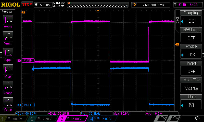
Fig. : LM5041B PUSH and PULL outputs
The overlapping of the PP outputs are of paramount importance for normal operation of CF-DIC stage and LM5041B has dedicated TIME pin used to define dead time (for Voltage-feed topologies) or overlap time (for Current-fed topologies) depends of how is RSET (R50) connected (to +Vcc or Gnd). The magnitude of the overlap time can be calculated as follows (RSET in kΩ):
Overlap time (ns) = (3.66 x RSET) + 7
Overlap time should be set experimentally: if too short it could jeopardize reliable operation and eventually damage at least PP switches, and if too long it results in increased output ripple since Cout cannot be charged during that time. With chosen R50 value of 15 kΩ the above mentioned equation gives us overlap time of about 62 ns. That is pretty in line with measured value of ~70 ns what can be seen on Fig. 10 and Fig. 11.
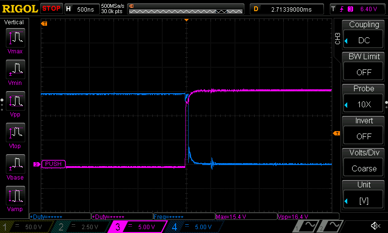
Fig. : PUSH-PULL overlap (PUSH rising edge)
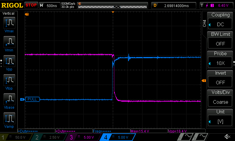
Fig. : PUSH-PULL overlap (PUSH falling edge)
Power transformer
The power transformer of any AC/DC converter represents an important component that demand special attention. The situation with CF-DIC power transformer is not different and comes with its own specific requirements. The first one is primary inductance (Lp) that should be as high as possible. In practice that requirement is limited by available core material and number of primary turns that is limited by physical dimension of the selected core. To meet that demand and still stay within reasonable transformer dimensions a VAC T60006-L2025-W380 soft magnetic toroidal core is selected made of VITROPERM 500 F material. It features extremely high AL of 67 µH that give us with only 28 primary turns a whomping 52.5 mH. That is in order of magnitude higher then what could be possible to achieve with the core of comparable volume made of any standard magnetic material. Huge Lp is beneficial for CF-DIC working since it doesn’t allow accumulation of huge amount of unused energy in the core. That results in small phase shift between current and voltage and small “duty loss”. Finally, that insure the reduction of the output “noise” (EMI).
Although the CF-DIC which is suitable for capacitive load, since it has a current source is series (i.e. two power inductors) is similar to flyback topology its transformer doesn’t need an air gap. Therefore the transformer utilization could be much higher in comparison to flyback hence it has better efficiency and require smaller dimension (volume).
The first power transformer prototype (Fig. 12) was winded literally in matter of few minutes, and it was behaved very well. Primary winding wires are twisted and inserted into heat-shink tube (black) before its winded on the core for improved HV isolation margin.
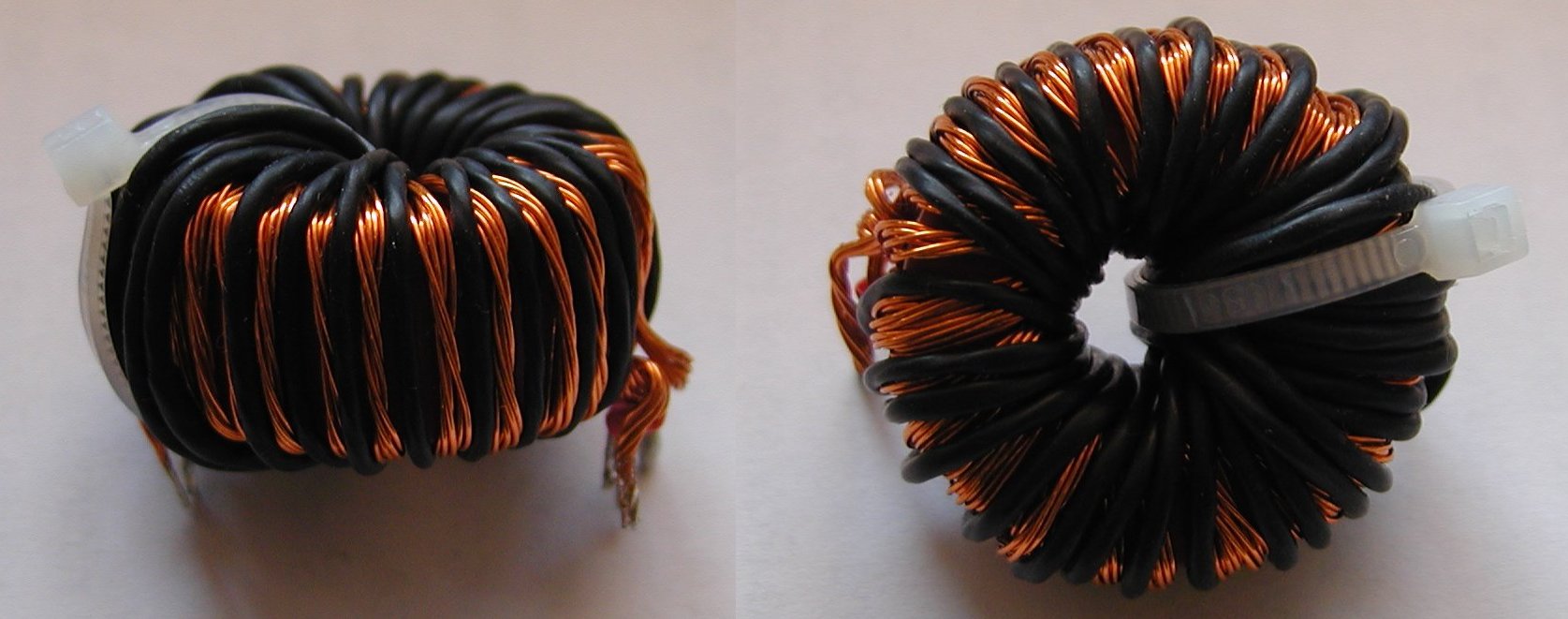
Fig. : The main power transformer first prototype
Thanks to Feryster (PL) the main transformer is made in professional manner and it’s fixed on the holder for easier mounting and soldering (Fig. 13).
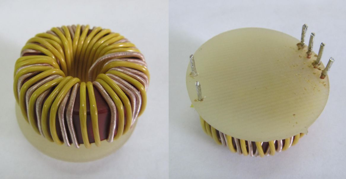
Fig. : The main power transformer custom made by Feryster
Protection circuits with shutdown
The over-temperature protection (OTP) is simply accomplished by monitoring NTC mounted on heatsink and compare it against voltage set by R58, R62 derived from LM5041B internal reference (+5 V). When set threshold is met, IC4B will trigger thyristor (Q4) that will shutdown LM5041B by connecting its UVLO input to the ground. It will remain in that state until power is recycled. If power is recycled too early, i.e. the NTC is still too hot, OTP will be instantly triggered once again.
The over-voltage protection (OVP) is aimed to limit max. output voltage which could goes far beyond max. operational range and easily destroy SR MOSFETs (Q7, Q8, see Fig. 17) in the first place. The Vds on them are defined by main transformer (TR3) ratio. For the 2:1 ratio Vds will be approximately twice higher then set output voltage (i.e. 50 V for 25 V output). Selected sync MOSFETs are rated for 150 V, therefore set output should never go over 75 V. For example, for output set to 52.5 V and Iout=5.4 A, Vds on the sync MOSFET looks like this:
Fig. : Sync MOSFET Vds for max output power
Usually in isolated converters the control signal (feedback loop) is applied to COMP input and FB is not used hence grounded. Here FB input is used to actively protect power converter by utilizing FB input if Vclamp voltage derived from push-pull stage (via D16, D19, C42) goes beyond set threshold, i.e. if R47+R48, R56 voltage divider gives more then 0.75 V LM5041B internal FB comparator will start to conduct and limit PWM duty ratio of HV buck stage. Therefore for set threshold of 130 V, the output voltage cannot exceed 65 V and Vds on sync MOSFETs cannot rise over 130 V. If output voltage is too high for longer then what is set by RC delay (R57, C53) the IC4A will trigger Q4 and power recycling is required to continue with operation. Of course if error condition is still active (i.e. large control voltage is applied, or tracker malfunction is happened) the OVP will trip again. For above mentioned example (Vout=52.5 V, Iout=5.4 A) the Vclamp present on C42 looks like this:
Fig. : Vclamp for max. output power
It’s a little bit higher then expected for 52.5 V measured on the output terminals (122 / 2 = 61 V) due to various losses (switching loses, voltage drop of output wiring, etc.) and Iout that is 5.4 A.
There is no doubt that in case of malfunction the output voltage could rise well over mentioned 75 V that will be fatal at least for the selected sync MOSFETs. That is especially true if higher Vin is applied (i.e. 230 Vac) when duty cycle for the max. output power is just about 22 % as shown on Fig. 16 (Hi-side MOSFET Vds).
IMPORTANT NOTICE: Never ever try to measure Vgs by touching HV buck Hi-side MOSFET Gate terminal. That is especially true for SiC MOSFETs that are so fast and sensitive that tiny capacitance of the scope probe is enough to couple voltage that will initiate multiple erratic switching that will almost for sure results in MOSFET damage that could be accompanied with explosion! Measure Vds that should follow the Vgs input instead.
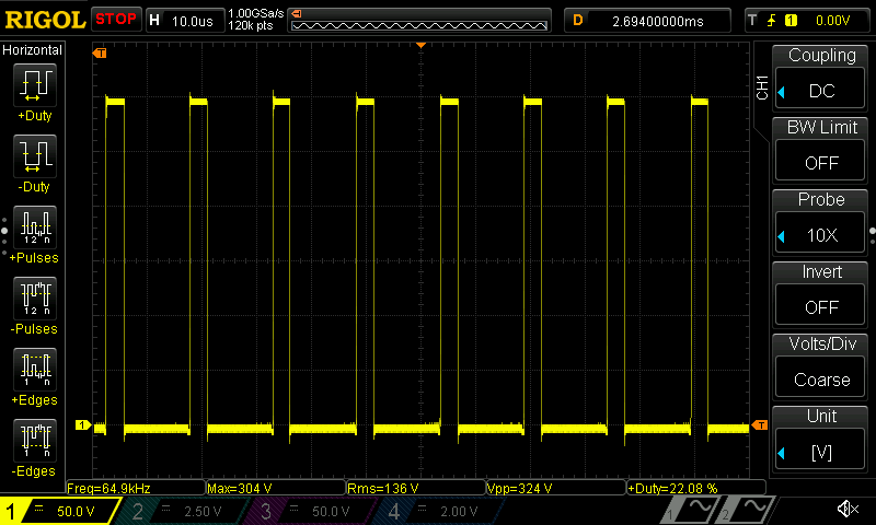
Fig. : HV buck output for max. output power
The OVP comparator circuit required a little bit more attention since boundary conditions such as start-up and applying huge load could induce false triggering. Therefore blanking circuit is added that consists of C54, D24, R65, C53.
Finally, if any of protection tripped and shutdown LM5041B (via ULVO pin), a red colored LED and open-collector output (nFAULT) will indicate fault condition and external control circuit (i.e. MCU and/or post-regulator) could be notified that something is happened. The nFAULT output is galvanically isolated (OK2).
Secondary side
Schematic diagram of the CF_DIC secondary side is shown on Fig. 17 That include synchronous rectifier, output capacitors and LC filtering, negative feedback loop (NFB) and tracker.
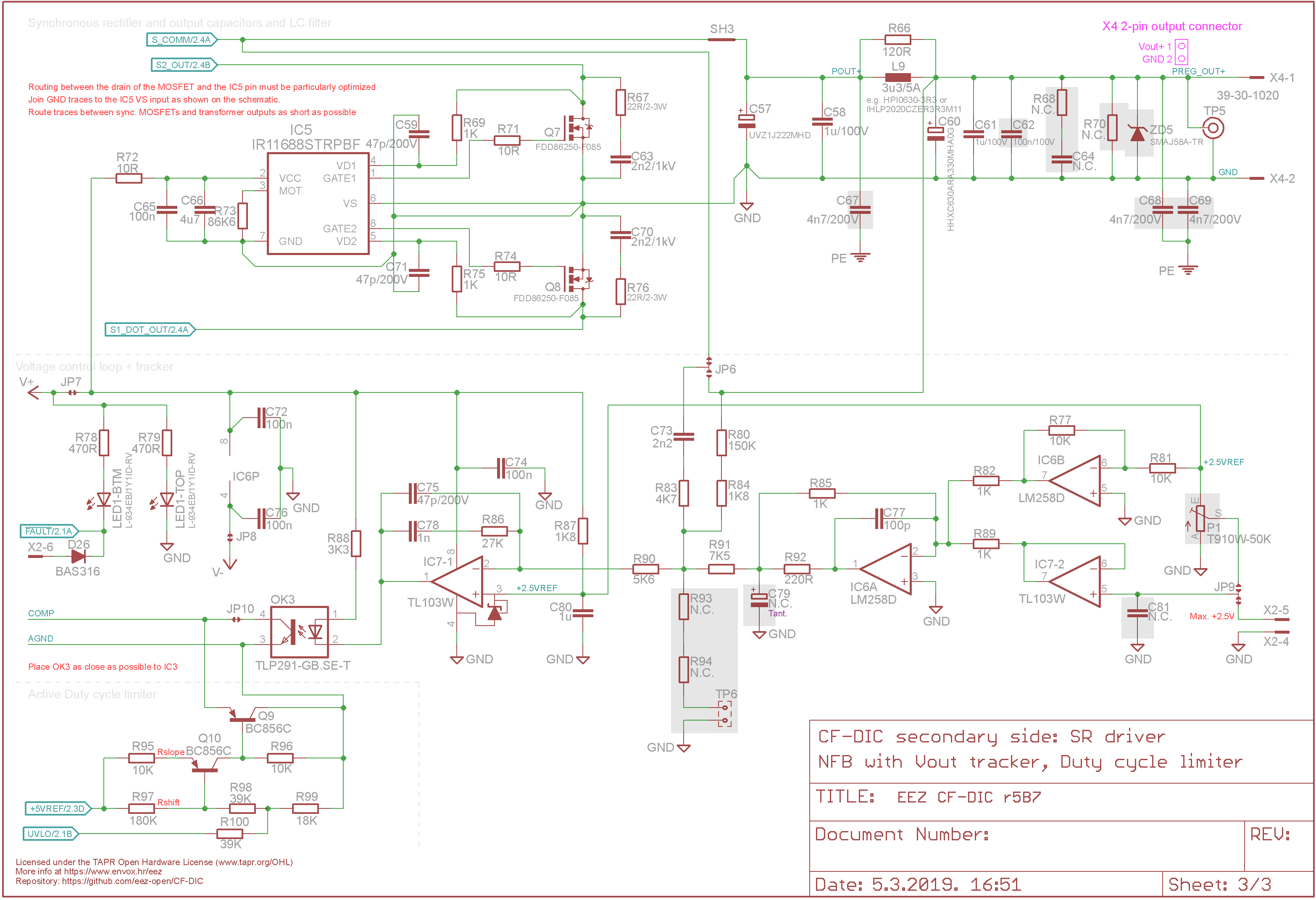
Fig. : Synchronous rectifier, NFB and tracker
Synchronous rectifier (SR)
The active (synchronous) rectification is chosen on the secondary side to improve efficiency. It is accomplished by deploying IR11688S (IC5), a secondary-side high speed 2-channel synchronous rectification controller for resonant half bridge converters that is able to directly sense MOSFET drain voltage of up to 200 V and operates with up to 400 kHz switching frequency. Importantly it can be also powered with Vcc as low as 4.75 V to 18 V that makes it suitable for +6.5 V available from the QR flyback main output.
Each IR11688S’ channel can drive one or multiple parallel MOSFETs to emulate the behavior of Schottky diode rectifiers, bypassing the body diodes for the majority of each conduction period to minimize power dissipation and remaining off during the blocking period. The Vds of each MOSFET is sensed to determine the source to drain current and turn each gate on rapidly at the start of each conduction cycle and off in close proximity to the zero current transitions for each branch of the output rectifier circuit.
Its programmable minimum on time (MOT) function provides flexibility to work over a wide range of switching frequencies. The cycle-by-cycle MOT protection circuit is able to automatically detect a light or no load condition so that the gate drives may be disabled to avoid unwanted reverse currents flowing through the MOSFETs.
Thanks to SR controller the whole circuit is rather simple: it include SR MOSFET with low Rds, on and appropriate Vds, max, its gate resistors, RC snubbers and output capacitors. The gate resistor value depends of selected MOSFET parameters and its calculated value of 3.3 Ω is set in accordance with calculation as suggested in manufacturer application note. The complete calculation can is available for the download at the end of this page.
Although for the SR purposes the selected MOSFETs often have Rds, on below 10 mΩ, they also usually have much lower Vds, max (100 V or lower) that is not suitable for our application. A good price/performance compromise is found in FDD86250_F085 that comes in DPAK package has reasonably low Rds, on of 22 mΩ and sufficiently high Vds, max of 150 V that give us margin of about 20 V in the worst case scenario.
The LC filter (L9, C60) follows the SR output to improve output ripple and noise figure. Optionally on the output terminals is possible to mount ZD5 for reverse voltage protection, bleeder R70 and EMI filtering capacitors C67, C68, C69.
NFB
The LM5041B works with closed control loop where output voltage is feed back to the COMP input using the error amplifier and opto-coupler. Usually for isolated control loops in switching converters with fixed output voltage a TL431 family IC is used due to its appealing price/performance. It is not deployed in this design since variable output voltage programmed from external source (e.g. post-regulator output voltage) demands additional circuitry that has to be harmonized with the operation of TL431. Therefore the TL103W is selected which is also intended for use in control applications of SMPS and linear power supplies. Its first operational amplifier (IC7-1) is used as error amplifier which compare control/feedback voltage present on its inverting input with fixed 2.5 V reference internally tied to its noninverting input .
The control voltage is derived directly from the converter output through voltage divider R80+R84 and R91. If we presume for a moment that tracker circuit is not present, and that the R91’s lower end is on the ground potential (0 V), the divider will set output voltage to the 53.1 V that represents the Vmax if feedback loop is functional and operates without oscillations. To insure stable operation two compensation networks are employed: C78, R86, C75 and R83, C73.
One important parameter in the feedback loop that require additional attention is opto-coupler LED’s current. It define, for given opto-coupler transfer ratio, how fast changes on the output will be transferred to the PWM controller (LM5401B), i.e. it participate in total loop gain together with NFB error amplifier (IC7-1) and PWM operational amplifier inside the LM5041B.
The following LTspice simulation (available for download at the end of the page) can give us an idea how value of RLED (R88) can affect operation of the LM5041B. We can start for example with value of 470 Ω that is, as we’ll see, too low, and that will result in high loop gain and over-sensitive response to any disturbance on the output – the circuit is unnecessary overreacting.
The simulation result is shown in Fig. 18. The reference voltage for error amplifier is 2.5 V therefore a small step from 2.4 to 2.6 V (green trace) is used to generate a disturbance (an regulation error). Blue trace displays how error amplifier (the LT1006 is used in the simulation instead of TL103W) will react with used compensation network and red trace show us what we can expect on the LM5041B’s COMP input. Please note that opto-coupler’s collector resistor (5 kΩ) is inside LM5041B what can be found in its datasheet (see Fig.3, pg.9). We can see that slope is too large, and that will cause a huge rise of PWM duty ratio for the HV buck. Consequently that will cause a huge change in output voltage.
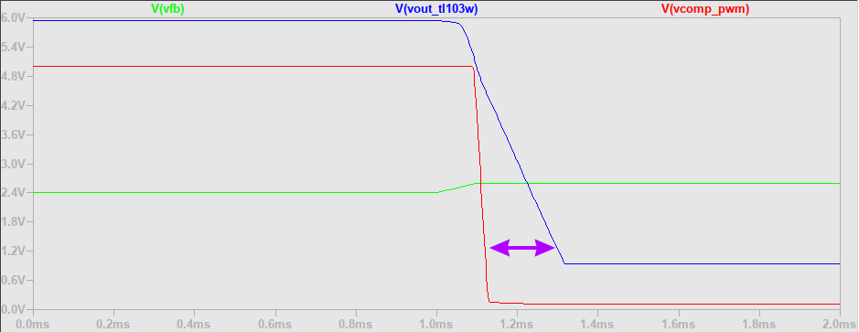
Fig. : Transfer ratio simulation for RLED=470 Ω
In the next step we can select another extreme RLED value of 10 kΩ that is too large and consequently max. LED current is too low. Now, the error amplifier will not be able to push PWM duty cycle down to zero. The LM5041B COMP pin cannot go below 3 V that is more then 50% duty ratio, what can be rather dangerous situation – for that duty cycle and high Vin of e.g. 240 Vac it will be way over max. Vout of 52.5 V (see Fig. 16). Note that LM5041B doesn’t need 0 V for 0 % duty, but it’s still well below 3 V.
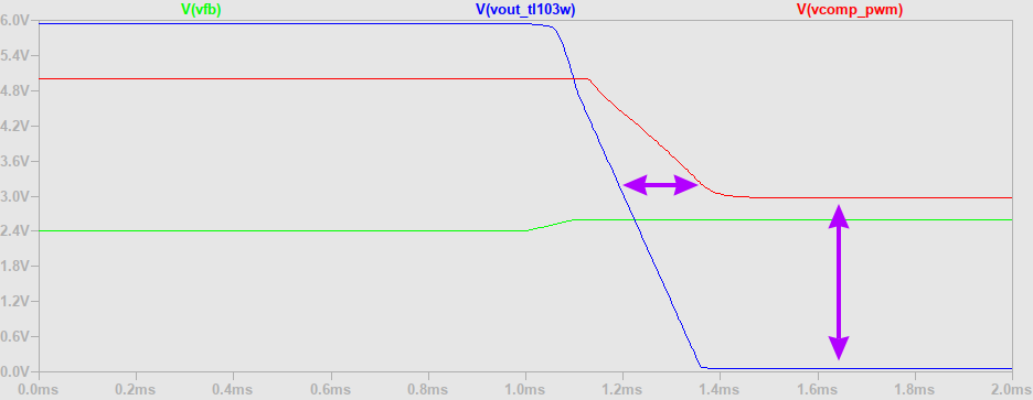
Fig. : Transfer ratio simulation for RLED=10 kΩ
Finally, we can see how this "transfer" works with selected value of 3.3 kΩ. It’s almost perfect – the PWM input (red) will almost 100% accurately follow the error amplifier response (blue) promising the most balanced operation.
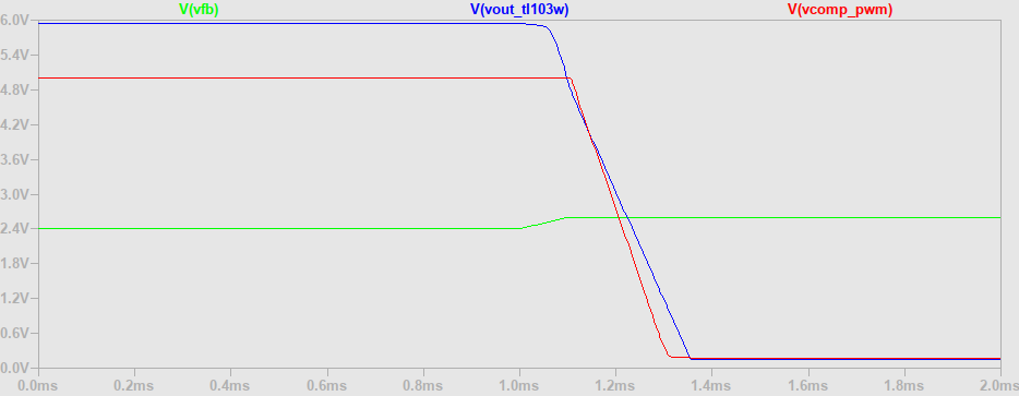
Fig. : Transfer ratio simulation for RLED=3.3 kΩ
Tracker
The voltage tracking circuit (or just tracker) is used to set/program converter’s output voltage to follow an external control voltage. Since the converter is designed to serve as power pre-regulator of a bench power supply in the first place, obviously that control signal should be derived from post-regulator output voltage. The tracker is using TL103W internal reference of 2.5 V. Therefore its control voltage ranges from 0 to 2.5 V. For example, if post-regulator circuit provides 0 – 50 V on its output, that has to be attenuated by factor of 20. The tracker function is to translate that control voltage to usable information for the error amplifier to drive LM5041B. Consequently the converter output will be adjusted between its defined limits that is about 2.5 and 52.5 V. The difference of 2.5 V over the whole operational range is the max. voltage drop that post-regulator circuit has to dissipate that remove a demand for huge heatsink and/or big cooling fan and improve overall power supply efficiency.
The tracker circuit can be rather simple, contains just one transistor (as in case of pre-regulator on the EEZ H24005 Power board). The main reason why such type of tracker is not implemented here is lack of linearity, i.e. the achieved voltage difference between post-regulator and pre-regulator outputs can vary depends of post-regulator’s output voltage and current from 2 to 4 V (e.g. 5 V or more at lower voltages, and below 2 V on the higher voltages and currents). Also it affects a AC response of the feedback circuitry that can result in unstable PWM duty cycle and eventually could cause erratic operation.
The chosen tracker is working differently by manipulating ground potential of the error amplifier control voltage divider. Since its operation takes into account stable voltage reference it can provide a pretty good linearity as shown on Fig. 21.
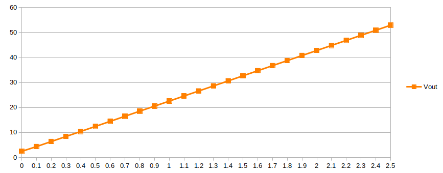
Fig. : Vout programming with tracker
The principle of operation of implemented tracker circuit is described in article Simple switchers make simple pre-regulators that include simple equation that has to be solved. It’s already mentioned that when the lower end of the R91 is connected to the ground the control loop will set Vmax at the output. But, if the potential on the lower end of the R91 increases, the output voltage will start to decrease and is set to reach 2.5 V for the full swing. The tracker operational amplifier gain has to be set to take into account max. control voltage (U_MON input), desired offset voltage between post-regulator output and its input (pre-regulator output) and voltage reference. In our case it has to be 1 since all of mentioned values is equal (i.e. 2.5 V). The tracker require negative voltage reference, that is provided by IC7-2. Since IC6 is dual operational amplifier, its second half is used for buffering of tracker input (U_MON) voltage. The optional P1 trimpot can be mounted, and PCB jumper JP8 modified for setting converter’ s fixed output voltage for applications other than power pre-regulator.
Downloads
IR11688 synchronous rectifier calculations for FDD86250_F085 MOSFETs
Opto-coupler transfer ratio LTspice simulation