Arduino Shield (digital control)
|
Current version |
r5B13a |
|
Status |
Completed, ready for production |
|
PCB manufactured |
Yes (r5B12) |
|
PCB assembled |
Yes (r5B12) |
|
BOM |
Yes (Farnell, TME, Digikey, Mouser, RS) |
|
File repository |
https://github.com/eez-open/psu-hw/tree/master/Arduino shield (include Eagle, Gerber and BOM files) |
|
License |
|
|
Contributions |
|
|
Revision history |
2017-11-04: r5B13a
2017-09-24: r5B13
2017-02-23: r5B12 (Version 3.0 on GitHub)
2017-01-11: r4B2
2016-12-11: r4B1
2016-10-24: r3B5
2016-07-24: r3B4 (Version 2.0 on GitHub)
2016-06-14: r3B3
2016-04-06 r1B14 (Version 1.0 on github)
2016-03-28 r1B13a
2016-03-27 r1B13
2015-12-07 r1B12b – First public release |
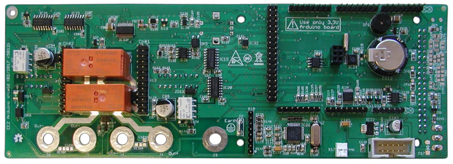
Fig. 1: Arduino Shield assembled (PCB r5B12, top side)
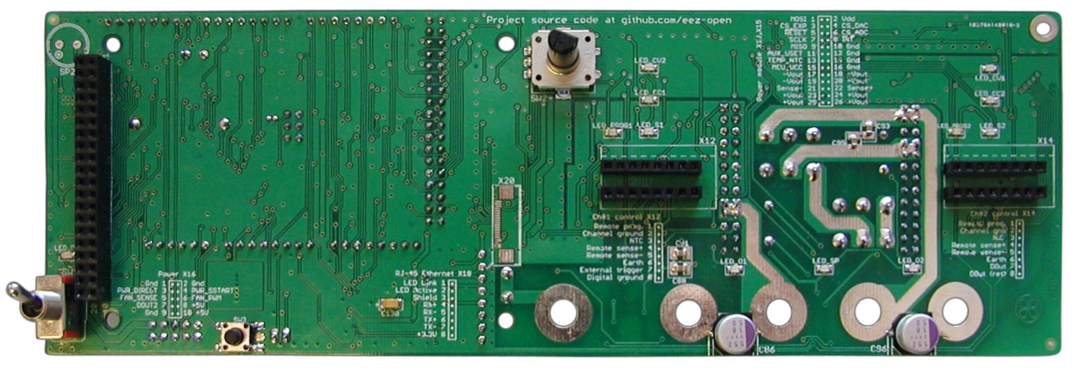
Fig. 2: Arduino Shield assembled (PCB r5B12, bottom side)
The Arduino Shield has three important functions:
- Carrying power output binding posts and remote sense inputs with the option to connect two output channels in series or parallel,
- MCU programming and supervision of up to two Power boards and
- Local user interface using TFT color touch-screen display
Additionally it offers the following functionality:
- Multiple LED status and operational indications
- Soft-start/Stand-by control (hosted on Auxiliary power module)
- MCU fan control (hosted on Auxiliary power module)
- EEPROM storage
- Real-time clock (RTC) with supercap back-up
- Reset supervisor with watchdog
- Beeper
- Analog inputs for temperature readings
- Ethernet communication
- Incremental encoder with switch
- Switching regulator frequency synchronization
- External digital trigger
- Power relay (DOUT2) control (hosted on Auxiliary power module)
- Optional audio amplifier and 20-pin FFC connector for 3.5” Riverdi TFT touch-screen displays
Binding posts section
This section has been added to simplify wiring of power binding posts, remote sense inputs, and serial and parallel connection control for the two channels without external wiring changes. Wiring of power outputs is controlled by the MCU firmware to reduce the possibility of an operator error, such as:
- channel output voltages and currents are not adjusted properly before connecting them in parallel,
- channel output polarities are mismatched or
- serial wiring is established while outputs are enabled that increase the risk of electric shock because of touching output when 50 V or more is present. An exceptionally dangerous situation since fire or electrocution is much increased at these voltages.
Output terminals have been located on the PCB so that direct mounting of 4 mm paired binding posts (with standard spacing of 19.05 mm / 750 mils) is supported. Power outputs are protected against reverse polarity and over-voltage spikes using TVS (ZD7, ZD10). Output capacitors (C87+R129, C89 and C92+R132, C94) required for both stable operation and lowered output PARD (ripple and noise) of Power modules are also mounted on the Power board PCB. For additional attenuation of PARD, C86 and C96 (elco-polymer, like OS-CON) are mounted in close proximity to the power output binding posts.
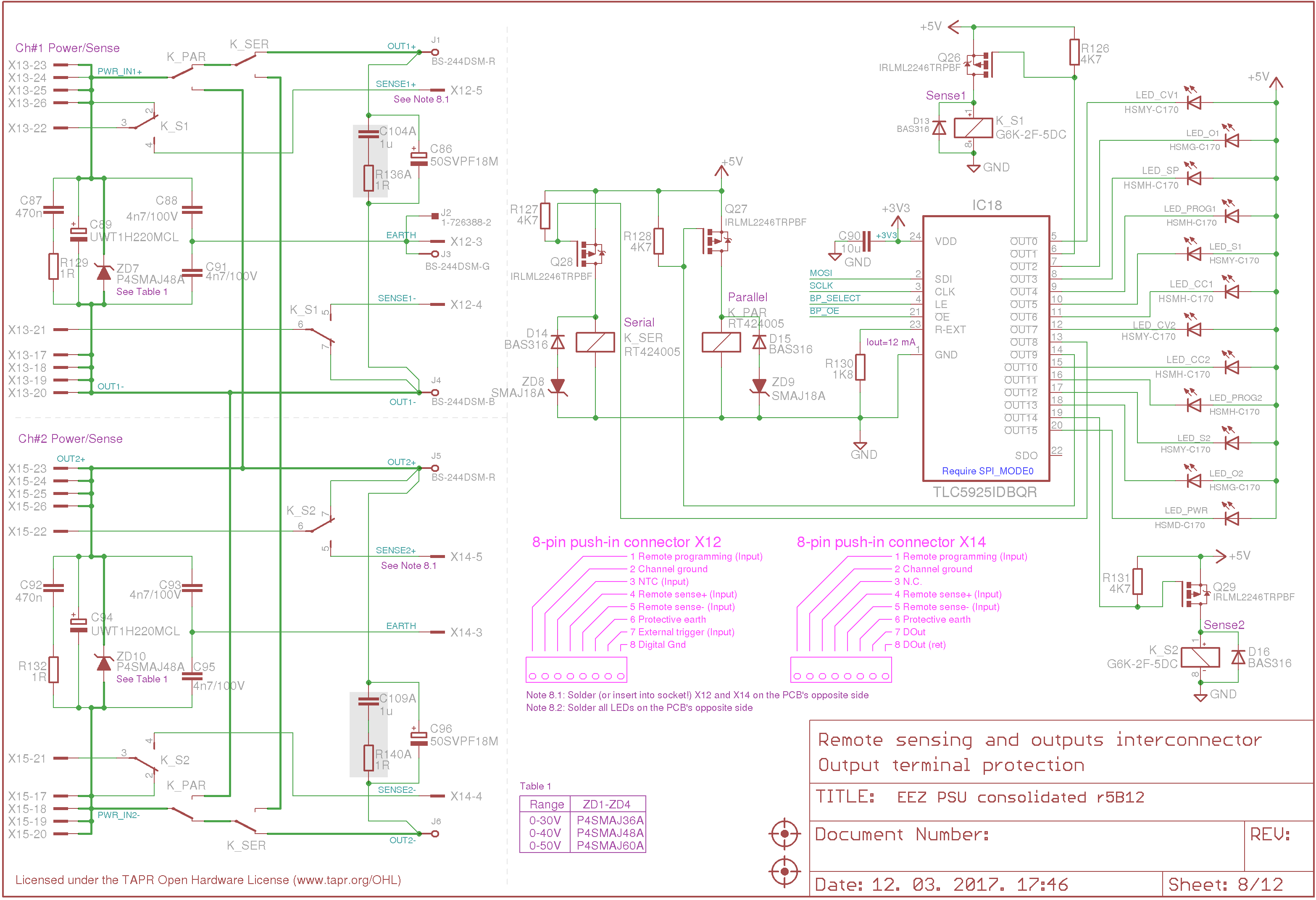
Fig. 3: Binding post section, relays and LED driver
Connecting two power outputs in series or parallel is done with two 8 A relays (K_SER, K_PAR). The channel outputs are separated/isolated when both relays are inactive; J1, J4 and J5, J6 binding post pairs are used for Ch1 and Ch2 respectively. When operating in either series or parallel, only two central binding posts (J4, J5) are used. This design choice was intentional to decrease the chance of bringing high voltage or current to loads already connected to either channel. In this way, the user need to physically move one or another wire to make a new operational scheme effective.
In addition, with this scheme with K_SER and K_PAR avoids the possibility of Power board damage due to a firmware bug that can activate both modes concurrently. The wiring in Fig. 4 makes clear that Parallel mode is more “significant” – when it’s selected it locks out the K_SER input contacts.
An obvious drawback of this wiring approach is disconnecting the C86, C96 capacitors when power outputs are coupled. Therefore, if lower PARD figure is still needed an external capacitor may be necessary.
When driving the serial or parallel relays, the following things have to be taken into consideration:
- Voltage and current must be zero before the channels are connected or disconnected. The easiest way to do that is to disable output (OE is off) but it’s also recommended to also program output values to zero.
- Coupling outputs in parallel is safely possible if programmed output voltages are the same on both channels
- Optionally, the down-programmer circuit could be disconnected on one of the channels when coupling in parallel is selected
Of course, wiring of two channels can be done independently of their built-in functionality. In this case, the recommendations above still apply.
Channel outputs, by default, are “floating” with regard to the PSU earth potential provided via a separate 4 mm binding post J3. This permits either negative or positive output to an external earth potential.
Note that with positive output connected to the Earth you should never take measurements with earth referenced instruments such as an oscilloscope. That will create a short circuit and excessive output current could damage the connected instrument’s wiring.
Remote sense is performed with signal relays (K_S1, K_S2), and local sensing is selected when they are not active. Activation of remote sensing is indicated with an LED (LED_S1, LED_S2); two additional wires (or perhaps a 2-wire shielded cable) has to be used to connect sensing inputs to the load. This technique is called Kelvin wiring and is common in high precision electronics work. Caution is required to avoid polarity mismatches. But, even if a polarity mismatch happens, a reverse polarity detection circuit on each Power board will limit output voltage, and an alarm for the MCU will be triggered.
All relays are indirectly driven (Q26-Q29) by a TLC5925 (IC18) which is a 16-channel constant current LED driver. A multiple output LED driver device was chosen because there are 12 LEDs used to indicate various condition during PSU operations:
- Power output is enabled (LED_O1, LED_O2, green, positioned between positive and negative binding posts on each channel)
- Power outputs are coupled in series (or parallel) (LED_SP, red, positioned between Ch1 negative, and Ch2 positive binding posts)
- CC limit mode (LED_CC1, LED_CC2, red, above push-in connector)
- CV limit mode (LED_CV1, LED_CV2, yellow, above CC LED)
- Remote sense is enabled (LED_S1, LED_S2, yellow, above the remote sense input pins of the push-in connector)
- Remote programming is enabled (LED_PROG1, LED_PROG2, red, above the remote sense input pins of the push-in connector) and
- Standby mode (LED_PWR, orange, between reset and the power switch)
All allowable binding posts connections with LED indications and programming codes that can be used for controlling the TLC5925 can be found here. Please note that the TLC5925 is powered with 3.3 V while all connected loads (LEDs and relays) use 5 V. This is not an issue for powering the LEDs because the TLC5925 outputs are constant current (max. current is defined with R130 or ~12.1 mA for 1.8 KΩ).
Arduino board
The Arduino Shield can work with any 3.3 V Arduino board. Currently, that means only one – the Arduino Due (two :)) which is a 32-bit ARM Cortex-M3 based board that comes in “Mega” form-factor. Hopefully more boards with the same form-factor will be available in the future from various Arduino designers (e.g. .org STAR – OTTO) or other sources. Connection with the Arduino board requires 8 connectors (Fig. 8): ICSP, DIGITAL, PWML, PWMH, ADCL, ADCH, COMM and POWER. They are located at the three board sides (with ICSP somewhere in the middle!); we learned that this arrangement is rather impractical when the board must be removed. Close attention is required to avoid bending one or more pins on the Arduino Shield side.
Controlling two channels and all peripherals used 64 I/O pins (SPI lines on ICSP connector were not counted) leaving “only” six pins available for future upgrades. Most of them (26) are assigned to the TFT LCD with its touch-screen display. Using another display with high speed serial interface can potentially reduce that to only 2 or 3 pins (+ SPI). An optional 20-pin FFC connector (X20) for 3.5” Riverdi TFT touch-screen displays is already available on the PCB as a possible migration path to a new more efficient local display solution.
Perhaps it’s worth mentioning that each additional Power board requires only four dedicated I/O pin for control. With existing pin mapping that give room for one additional channel (of course that will also require a new PCB layout). The newly introduced 16-bit I/O expander on the Power board (r5B12) could reduce this to only two I/O pin (+ SPI that is currently shared between all peripherals). The pin mapping of all used pins is described here.
Input power of the Arduino Shield is +5 V, supplied by X16 from the Auxiliary power module. The Arduino Due is a 3.3 V board, but 5 V is used as its power input. It can be powered via the POWER header 5V pin (or from a USB port). An internal 3.3 V LDO regulator is used to adjust the 5 V to 3.3 V for local on board use. That LDO is not used for powering 3.3 V circuits on the Arduino Shield. An additional regulator is used for that purpose (IC22).
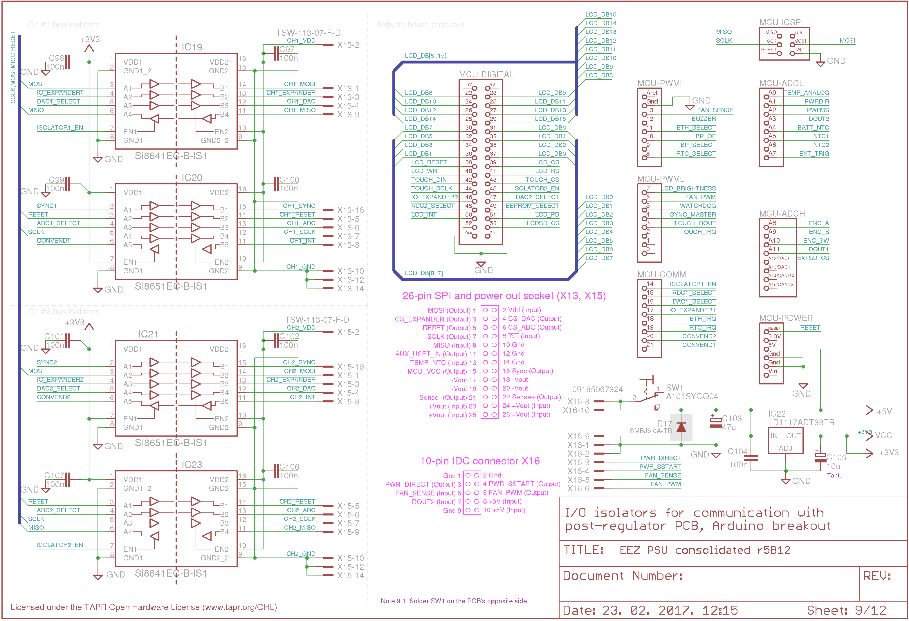
Fig. 4: Digital isolators, 3.3V LDO and Arduino board connections
Digital isolators
The Arduino Shield can control two PSU channels which are electrically isolated by default; they must remain isolated when they are connected to the Shield. That means digital control signals cannot share the common ground. If such a connection occurs (perhaps via an accidental short), it could be even dangerous when, for instance, channel outputs are connected in serial or when the PSU is used as a dual rail source (positive output from one channel is connected to the another channel’s negative output). Digital channel isolation is accomplished using high speed Si86xx series digital isolators.
Two digital isolators are used per channel to isolate 7 outputs and 2 inputs (IC19, IC20 for Ch1 and IC21, IC23 for Ch2). They are SPI lines, chip selects for SPI peripherals on the Power board (ADC, DAC and I/O expander), and Master sync for switching regulators frequency synchronization. The MISO line (Master-in-Slave-out) SPI line requires additional control (ISOLATOR1_EN, ISOLATOR2_EN outputs) to select receiving of data from one channel at a time. Otherwise, data corruption will be inevitable.
Power board I/O connector
Two 26-pin headers (X13, X15) are used to connect with the Power boards. Functions of the first ten pins follows the ICSP 10-pin header mapping carrying digital signals for SPI, chip selects and supply voltage for the channel side (B side in accordance to Silicon Labs datasheet) of the digital isolators. The rest of the connector is used for various analog signal and power lines as described in table below.
|
# |
I/O name |
Active |
Description |
|
1 |
MOSI |
High |
MOSI (SPI) |
|
2 |
Vdd |
Power |
Power board +5 V output |
|
3 |
CS_EXPANDER |
Low |
I/O expander chip select |
|
4 |
CS_DAC |
Low |
DAC chip select |
|
5 |
RESET |
Low |
Reset |
|
6 |
CS_ADC |
Low |
ADC chip select |
|
7 |
SCLK |
High |
SCLK (SPI) |
|
8 |
INT |
Low |
I/O expander IRQ / ADC conversion end |
|
9 |
MISO |
High |
MISO (SPI) |
|
10 |
Gnd |
Power |
Power board ground |
|
11 |
AUX_USET_IN |
Analog |
Remote voltage programming |
|
12 |
Gnd |
Power |
Power board ground |
|
13 |
TEMP_NTC |
Analog |
Power board temperature sensor (NTC) |
|
14 |
Gnd |
Power |
Power board ground |
|
15 |
MCU_VCC |
Power |
Arduino board +3.3 V output |
|
16 |
Sync |
High |
Master sync for switching regulator’s frequency synchronizations |
|
17 |
Vout- |
Power |
Negative power output |
|
18 |
Vout- |
Power |
Negative power output |
|
19 |
Vout- |
Power |
Negative power output |
|
20 |
Vout- |
Power |
Negative power output |
|
21 |
Sense- |
Analog |
Remote voltage sensing negative signal |
|
22 |
Sense+ |
Analog |
Remote voltage sensing positive signal |
|
23 |
Vout+ |
Power |
Positive power output |
|
24 |
Vout+ |
Power |
Positive power output |
|
25 |
Vout+ |
Power |
Positive power output |
|
26 |
Vout+ |
Power |
Positive power output |
I/O peripherals
SPI peripherals might be added to the Arduino Shield (Fig. 8) to provide functions are not regularly available on the Arduino board. In fact, for the Arduino Due that is partially true because its MCU has RTC (Real-time-clock), and even Ethernet. But as far as we know, the former cannot be easily powered from a back-up source when the main power is switched off, and the latter is not exposed to an external connector nor supported through Arduino libraries. The on-board RTC (IC24) supply is backed up with 1 F Supercap (C112) which should be enough for keeping it running for a couple of weeks when the main power is not present.
Ethernet communication is accomplished using (IC26). In addition, an EEPROM (IC25) is added since MCU on Arduino Due does not have any EEPROM memory.
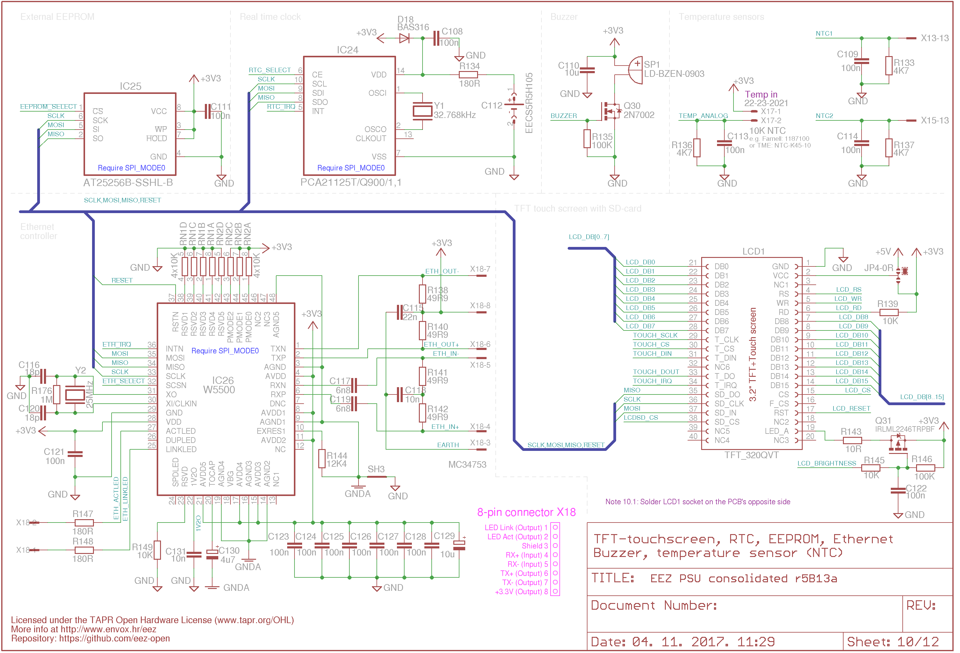
Fig. 5: Arduino Shield peripherals
The TFT display (Fig. 6) has 3.2” diagonal size, 262K (18-bit) colors and 240 x 320 pixels (rotated horizontally!) that gives enough room to display much important information about both channels and system status and messages simultaneously. Color coding could improve the visibility of one or another value amongst the data from various sources. This display unfortunately is not available yet through major suppliers mentioned in the BOM, but it can be easily found on any major on-line shopping site (eBay, AliExpress, etc.) by searching for TFT_320QVT. Additionally, the search query could be further narrowed by physical size (3.2 Inch), resolution (240 x 320), and the name of the matching LCD controller (SSD1289). The newer display version comes with a new LCD controller (ILI9341); the PSU firmware supports both versions.
This display also comes with SD card slot that can be used as mass storage for such things as data logging, user’s programs, data, etc.
A few words about selection of SPI bus. It’s very common for devices with similar functionality and complexity as the EEZ PSU to use an I2C bus for communication with various peripherals. Devices with such interfaces are in general cheaper, require only two lines for communications (no SCLK and no dedicated chip select for each device is required!), and are well supported with software libraries. I2C can be very beneficial for low end MCUs with low I/O pin count. But that also in general means less processing power and memory which makes them unsuitable for the firmware complexity we need. We have already mentioned that the Arduino board we recommend offers enough I/O ports for addressing 16-bit TFT LCD, various peripherals, and at least two Power board (up to 3, or 4 if SPI is used for touch-screen controller). Anyway, SPI bus offers more flexible device addressing and much faster communication which makes the PSU more responsive.
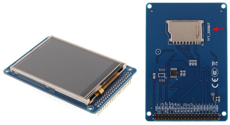
Fig. 6: 3.2" Color TFT display with touch screen and SD-card socket
Not all peripherals requires SPI nor any other mean of digital bus interfacing. Such examples are:
- buzzer (SP1) that is driven with PWM output (via Q30),
- analog inputs for temperature sensors (TEMP_ANALOG, NTC1, NTC2 inputs),
- isolated analog input for temperature sensor (BATT_NTC, see Fig. Error: Reference source not found),
- TFT display backlight adjustment driven with PWM output (via Q31),
- incremental encoder (ENC_A, ENC_B, see Fig. Error: Reference source not found)
- external digital trigger input (EXT_TRIG, see Fig. Error: Reference source not found) and
- power relay output (DOUT2)
SPI modes
Working with SPI peripherals requires selection of the mode of operation. Four modes are available and defined by serial clock (SCK or SCLK) polarity and phase. For example the Arduino IDE provides four data constants for them: SPI_MODE0, SPI_MODE1, SPI_MODE2 and SPI_MODE3. Selecting a right mode of operation can be frustrating when IC manufacturers specifications or hardware implementation are unclear. We learned that if an IC is not damaged or improperly connected but IC response is erratic, checking the SPI mode in use is the first thing that should be done! If you are not sure what mode to use, the fastest way to establish meaningful communication is to simply select them one by one and monitor the results (i.e. the outputs are set correctly, or the returned data register content is equal to the one that has been set, etc.).
Remote communication
The EEZ PSU can communicate with the external world using USB or Ethernet. The on-board Ethernet controller (IC26) is only missing a RJ-45 modular jack for a LAN cable connection. The connector is to be placed on the Auxiliary power module which is in turn mounted directly on the inner side of the enclosure’s rear panel. The USB-B connector is similar – it’s located near the Ethernet RJ-45. It is not connected to the Arduino Shield, but rather directly to the Arduino Due’s USB programming port. A 5-pin to micro-USB cable (as shown in Fig. 7) is used.
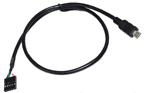
Fig. 7: Micro USB to 5-pin cable
Supply-voltage supervision, watchdog and reset
A TPS3705-33 (IC31) is used to improve overall reliability of the PSUs digital controls, and provides the following functions:
- Supervises the 3.3 V supply provided by IC22 (Fig. 8), and generates a 200 ms RESET pulse on power up and power fail,
- Provides a “clean” (i.e. well defined) reset when manual reset tactile switch (SW3, Fig. Error: Reference source not found) is used and
- Generates reset if the MCU, due to hardware or firmware issues, misses sending a WATCHDOG signal within 1 second.
The reset signal generated by IC31 is also used to immediately deactivate main power by pulling down the control outputs (PWR_DIRECT, PWR_SSTART) of both triacs on the Auxiliary power board via IC29 as additional precautionary measure against unexpected conditions. The same scheme is used with the power relay DOUT2 control.
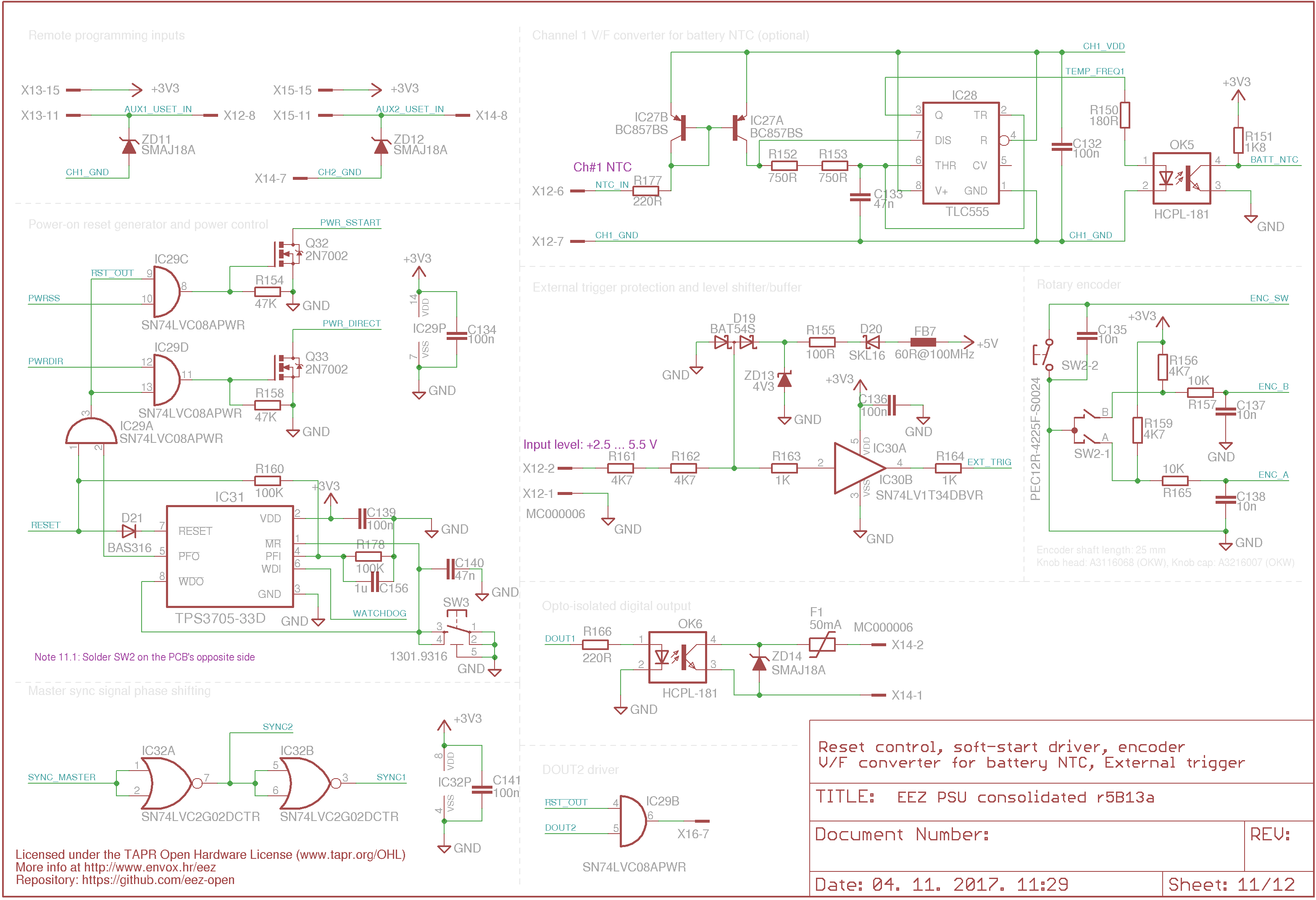
Fig. 8: Reset supervision, master sync phase shifter and various non-SPI periperals
Special I/O
The Arduino Shield has two special inputs that can be used for external control of the PSU. Both inputs are wired to the X12 8-pin push-in connector above the Ch1 binding posts. The first is an analog input which can be used with a 10 kΩ temperature sensor which is the standard value for batteries which has a temperature monitoring output. In addition to monitoring battery during fast charging, it can be used to controlling PSU’s channels for different sources. The BAT_NTC output is a digital output (the popular 555 timer, IC28, acts as a Voltage-to-Frequency converter) because it’s easier to isolate it while maintaining good accuracy then an analog signal. For better linearity, the input resistor is not connected directly to the timer, but to a current mirror circuit is used (IC27). R177 is used to limit current in case the NTC input are incidentally shorted to ground (if such a fault condition lasts for a prolonged period, that could cause loss of PWRGOOD signal on Ch1 upon which firmware will push the entire PSU into standby mode). OK5 is used as an optical isolator.
Another input is purly digital and can be used for triggering various PSU’s functions via an external digital signal which can be connected, for example, to a D.U.T. An MCU input is used for connecting external signal but the connection is not direct – direct connection to some external signal can easily induce erratic behavior or even irreversible damage in the MCU! Therefore, the MCU input is protected against over-voltage and reverse polarity conditions with D19 and pre-polarized ZD13. R161-R163 limit current to the protection circuit, and IC30 behaves as a buffer and level-shifter. Finally, R164 limits the current that can be drawn by the MCU input. Thanks to the level-shifting feature, an input signal can be anything between approx. 2.5 and 5 V and still work properly.
The DOUT line is an opto-coupled (OK6) and protected (F1, ZD14) MCU output that can be used for triggering external devices.
Switching regulators frequency synchronization
The PSU has two switching pre-regulators which, without synchronization, will work with different switching frequencies. That could increase EMI (i.e. radiated noise from the PSU) and can result in higher ripple and noise on its outputs. As a result, frequency synchronization can be supported in firmware. When selected, the “master clock” is generated by Arduino Due (SYNC_MASTER, Fig. 8) and distributed to switching pre-regulators on the Power boards. The master signal (SYNC_IN) then arrives at a Power board via IC32: as SYNC1 for Ch1 and intentionally inverted SYNC2 for Ch2. Switching noise on a channel outputs will be 180o out of phase which should decrease total noise energy radiated, especially when both channels are coupled in parallel.
A two layer PCB (220 x 74 mm) holds not only the Arduino board but also the TFT LCD, all the binding posts, the LEDs, switches and plug-in connectors. The board was laid out in Eagle, but the autorouter was not used. In that way, only three cables are required to connect with the rest of the system. Power board connectors (X13, X15), power input (X16), and Ethernet (X18) are soldered on the top side of the board. Binding posts (including protective earth), LEDs, switches and push-in connectors are soldered on the bottom side.
The distance between the PCB and the enclosure’s front panel is 18 mm, therefore the binding posts we’ve selected cannot be connected directly to the connection points on the PCB. A screwed spacer sleeve mentioned in the BOM has to be used. See the building instructions.
Some parts are located in the area beneath the Arduino board (e.g., RTC, or EEPROM), therefore they have to be soldered before the Arduino is plugged in.
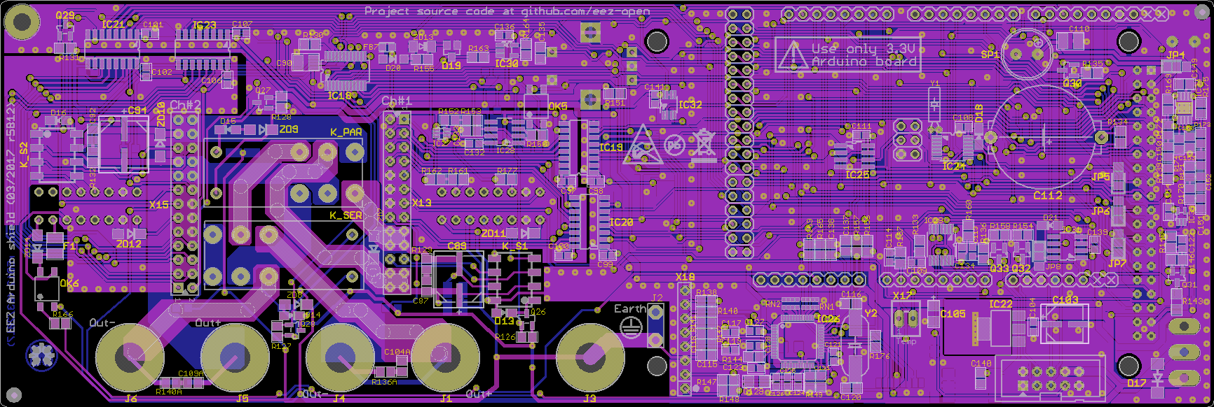
Fig. 9: PCB layout r5B12 (both sides)
For possible modifications and tweaking visit the Hacking area.