DCP405 module measurements
DCP405 module measurements
Load transient response testing using MOSFET switch
The load transient response illustrates a power supply’s ability to respond to abrupt changes in load current. The simplest way to achieve that is to use a MOSFET as a fast switch that will connect an additional load in parallel, increasing output current. The output voltage is shown on the scope image in yellow trace and the voltage on the MOSFET input in blue.
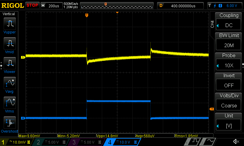
Fig. 1: Load transient response tested with MOSFET switch
Load transient response testing using a closed loop load transient tester
Load transient response (or recovery) can be measured more accurately using the dedicated tester described here. Additionally, remote sensing has to be deployed and oscilloscope probe has to be applied on the power output terminals. Result is shown in Fig. 2 for step load of 1 A, while output voltage was 12 V.
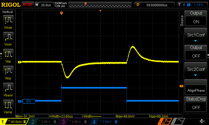
Fig. 2: Transient response measured with load tester
Short circuit recovery
Testing short circuit can be also done using the MOSFET switch, but that is directly connected to the power supply’s output terminals. The output voltage is set to 6 V. The output current is also set to a maximum value of 5 A. On Fig. 3, the yellow trace is the output voltage, and the blue trace the MOSFET gate signal. Measured recovery from a shorted output is below 2 ms.
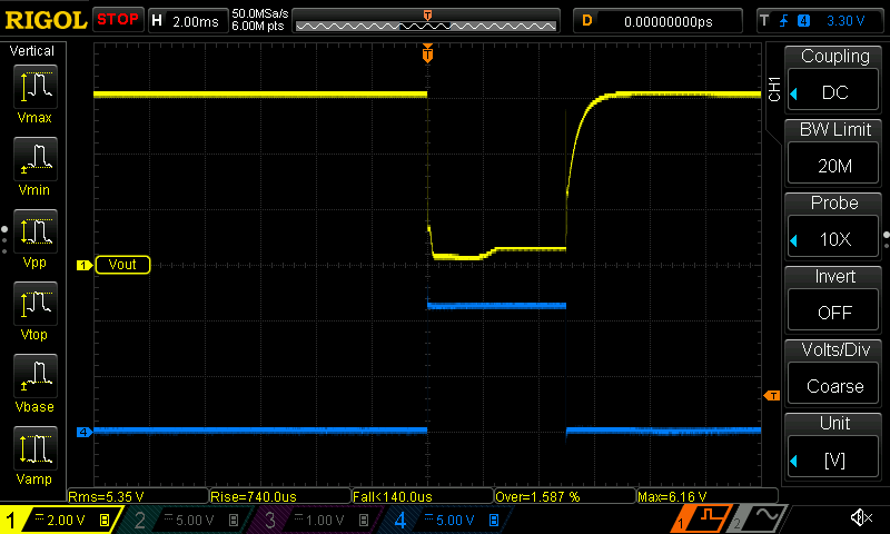
Fig. 3: Short circuit recovery
Capacitive load
The Capacitive load testing is performed by simply connecting a capacitor to the output terminals with oscilloscope probe already connected, A huge output voltage drop is expected from an uncharged capacitor. Fig. 4 shows what happened when the output voltage is set to 30 V and a 10 000 μF electrolytic capacitor is connected. The output after recovery remains stable, without sign of oscillation.
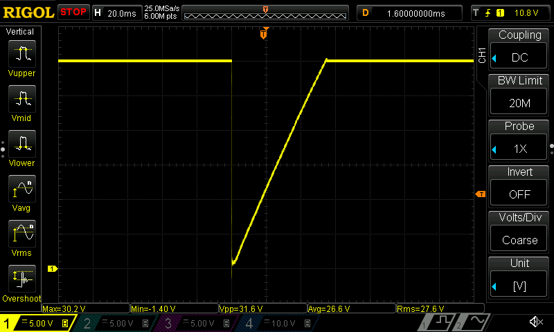
Fig. 4: Output voltage drop when a 10 000 μF uncharged capacitor is connected
When down-programmer is present and activated (that is a default for the DCP405 module) it is important to check how it behaves with huge capacitive load connected while programmed output voltage varies. Fig. 5 shows voltage that output voltage rises and falls without visible oscillations when 2200 μF is connected on the output and no resistive load is presented. The down-programmer needs only 20 ms to discharge such huge load (charged to 30 V). It has to dissipate that in heat. Therefore performing such testing with high frequency will rise the main heatsink temperature considerably, but MCU will acts by increasing cooling fan speed accordingly.
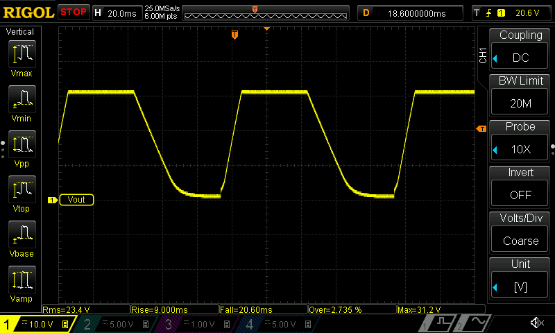
Fig. 5: Charge and discharge of 2200 μF capacitor (Down-programmed enabled)
Inductive load
The DCP405 module behavior with the connected inductive load is tested by repetitively applying 100 μH power inductor using once again the MOSFET switcher. Output voltage is set to 30 V and current to 5 A. Power output (yellow trace) does not shows any sign of oscillation.
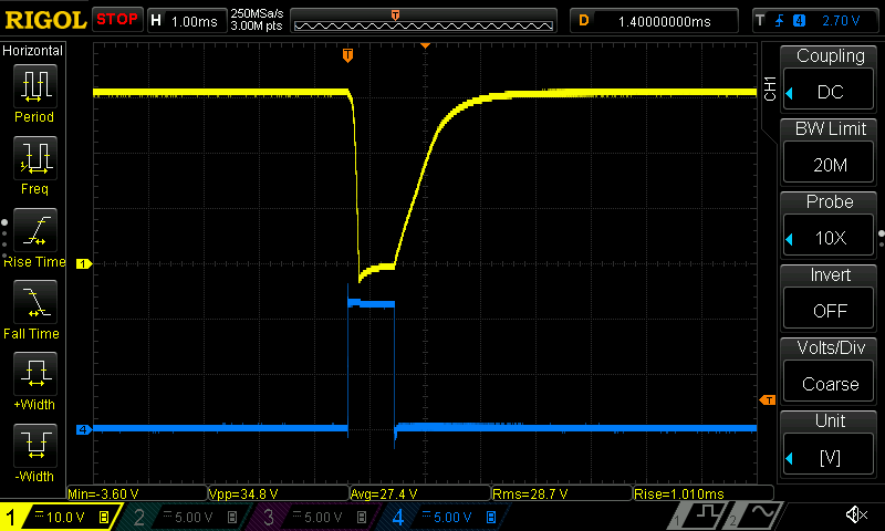
Fig. 6: Output voltage with 100 μH inductive load connected
Output voltage programming (internal DAC)
Testing the output voltage programming can demonstrate undesirable overshoots or undershoots when the output voltage is changed rapidly. In addition this test can give us an idea of responsiveness of the complete system (i.e. power supply firmware, and the settling time of the output). The result shown in Fig. 7 was generated by step change the output voltage from 5 V to 40 V, with no load connected. The programming period is just 6 ms (167 Hz).
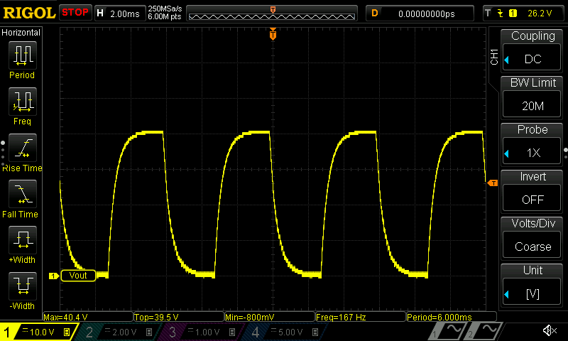
Fig. 7: Fast programming (via SCPI LIST), full range, no load
The rising time without load connected for full range step (i.e. 0 to 40 V) is shown on Fig. 8. and falling time (with down-programmer activated) on Fig. 6.
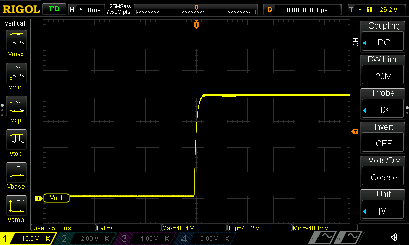
Fig. 8: Output voltage rising time (no load, full range)
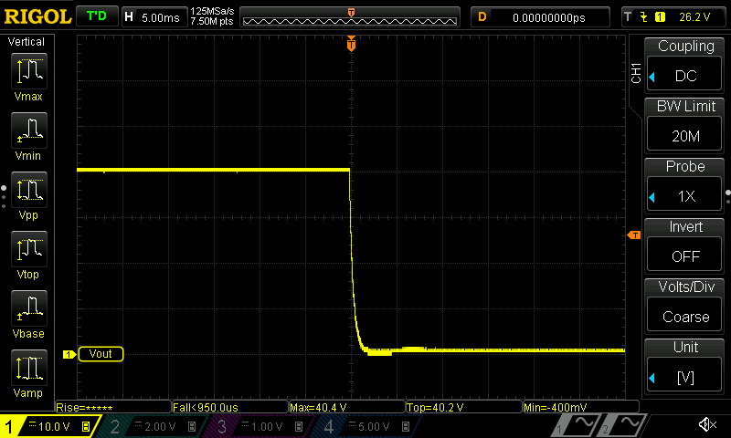
Fig. 9: Output voltage falling time (no load, full range)
Output voltage programming (external signal source)
The DCP405 power module can be also programmed from an external source using the protected input accessible via the front panel push-in connector. As in the case of internal programming, +2.5 V is required for full scale. In this operating mode it is possible to measure the maximum settling time because the input analog control signal is applied directly to the CV control loop.
A square wave and sine wave programming external signals are used to get results shown in Fig. 10 and Fig. 11. Since sine wave programming could goes up to 400 Hz it could be used to emulate ripple of fully rectified mains ripple (i.e. 100 or 120 Hz).
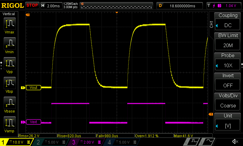
Fig. 10: Output voltage programming from external source (100 Hz square wave)
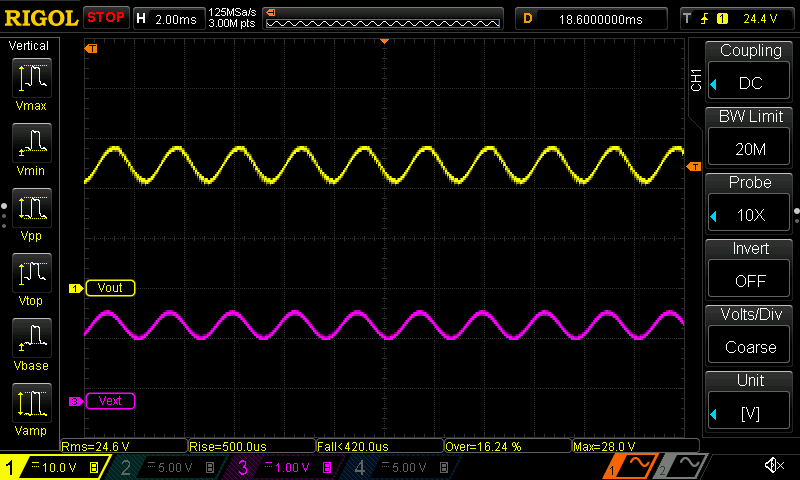
Fig. 11: Output voltage programming from external source (400 Hz sine wave)
Change the mode of operation (CV/CC)
The DCP405 changes its operational mode when a particular programmed output value is reached. A sudden change in resistance that could change a mode of operation must be “smooth” – no oscillation nor overshooting are permitted during a transition. This test was performed by repetitively connecting and disconnecting an additional load with a MOSFET switcher driven by the signal generator (blue trace). The output voltage was set to 40 V and current limited to 500 mA. Therefore when the right load is applied, the DCP405 module should change mode from CV to CC which will cause the output voltage to drop as shown on Fig. 12.
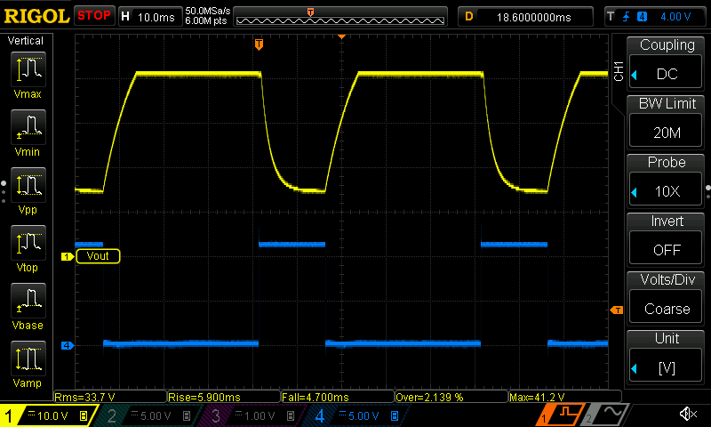
Fig. 12: Mode of operation changes
Power on, forced power off, standby and soft reset
When the power module is powered on or off, the output voltage should show no signs of overshoot. Powering on with output voltage set to 30 V is shown on Fig. 13. and powering off on Fig. 14.
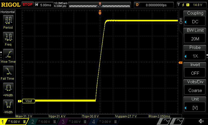
Fig. 13: Power on, Vout=30 V, no load connected
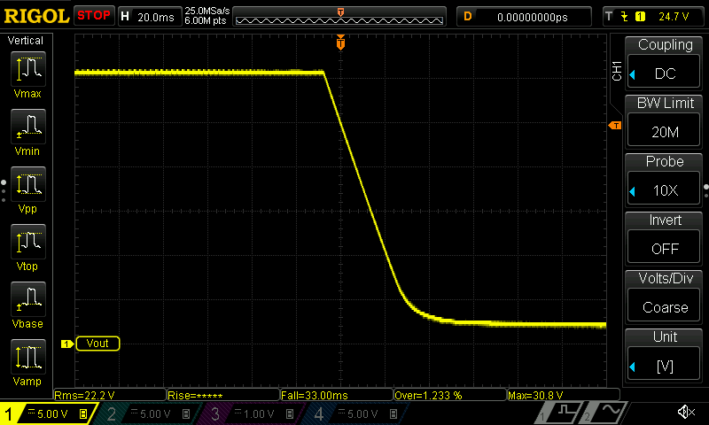
Fig. 14: Power off (AC main unplugged), Vout=30 V, no load connected
Entering standby mode is equal to powering off but preformed under firmware control. Therefore its possible to disable power output first and then remove the input power. The results is visible on Fig. 15.
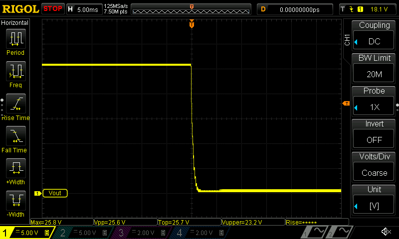
Fig. 15: Entering the stand-by mode, Vout = 25 V, no load connected
Executing soft start is similar to standby mode but without removing input power. Therefore the output voltage drop is even faster since post-regulator control circuits remain functional, output voltage is set to zero, and output capacitor discharge is assisted by down-programmer (Fig. 16.).
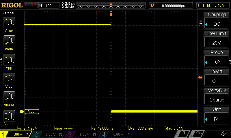
Fig. 16: Output voltage drop on soft reset
Down-programmer
The down-programmer circuit rapidly draws off the energy stored in the output capacitor and connected device’s input capacitor. Effectively, it sinks the current from the capacitors back inside the power module where it is dissipate into heat. If programmed voltage drop in short period of time (tens of milliseconds) is large (e.g. 30 V to 0 V), the output voltage without down-programmer cannot be set as it is shown in Fig. 17. The same voltage drop can be easily accomplished with down-programmer circuit enabled (Fig. 18.)
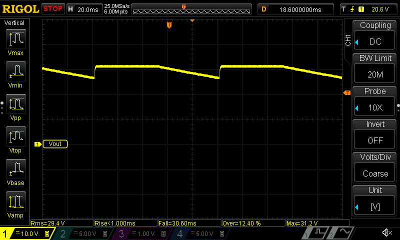
Fig. 17: 30 V step without load and down-programmed disabled
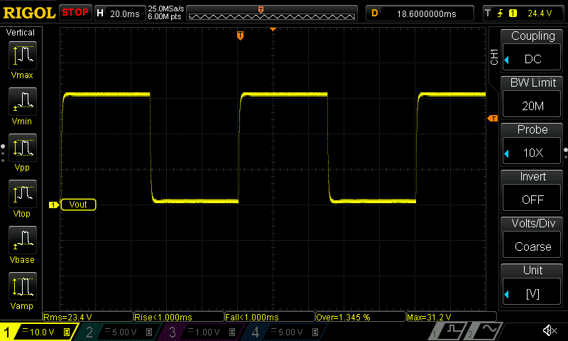
Fig. 18: 30 V step without load and down-programmed enabled
HW (crowbar) OVP
The DCP405 module comes with both software and hardware OVP (over-voltage protection). The response time of the software based OVP is limited by the execution speed of firmware that take care of all modules and has to periodically check if set OVP threshold is reached or not. It could be too slow when protection of the sensitive connected device is needed that cannot tolerate more then few percents over its nominal supply voltage.
Operation of the hardware based OVP on the other side is not affected with other tasks that MCU has to accomplish since it is accomplished by dedicated circuit to monitor output voltage. Therefore it can act as fast as that circuit can reacts (i.e. its crowbar element in the first place).
Hardware OVP circuit has fixed threshold level that is set to approximately 5% above programmed output voltage. On Fig. 19, the output voltage is set to 30 V and “error” voltage of 31.5 V is applied from external source on the DCP405’s power output terminals. The response time is within 20 μs that is almost two order of magnitude better then software based OVP. The similar response time of about 30 μs can be measured for lower set output voltage, e.g. 3.3 V as shown on Fig. 20.
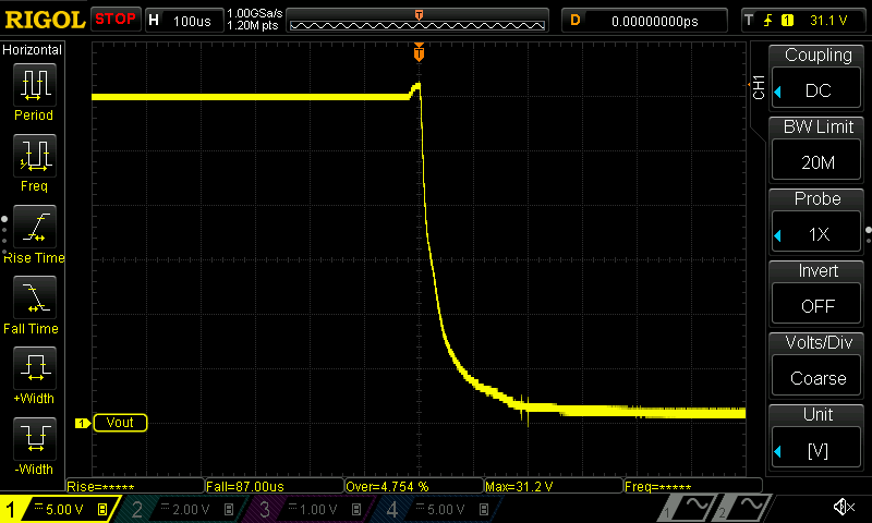
Fig. 19: OVP tripped on Vout = 30 V
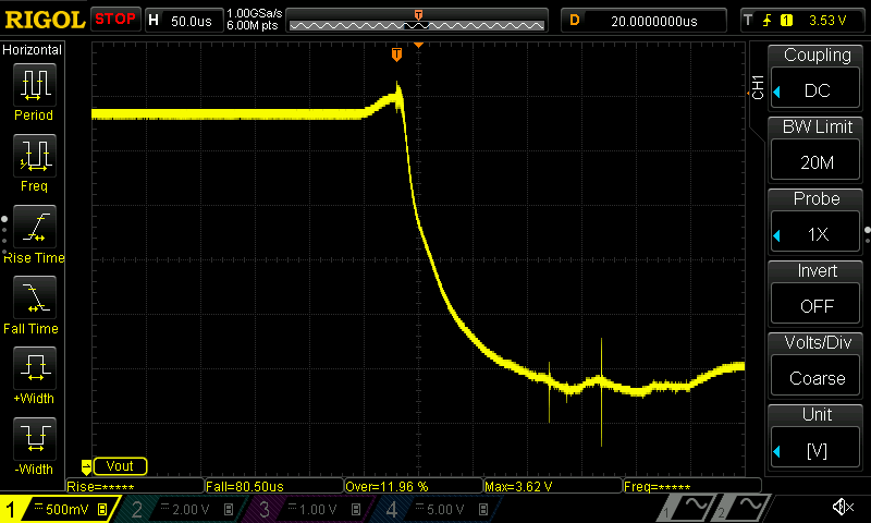
Fig. 20: OVP tripped on Vout = 3.3 V
Output ripple and noise (PARD)
The PARD (Periodic and Random Deviation) that exists on the power output is caused mainly by switching power pre-regulator and to some extent by bias power supply noise because the post-regulator circuit has limited ability to reject such switching noise. Since PARD consists of low level, broadband signals, major test set concerns are ground loops, proper shielding, and impedance matching. PARD measurement setup is shown on Fig. 21. To block the DC current a 4.7 μF capacitor is connected in series with the signal path, and to eliminate cable ringing and standing waves 50 Ω in-line terminator is used. Protective Earth (PE) of DSO and power module are directly connected to reject common mode noise as shown on Fig. 22.
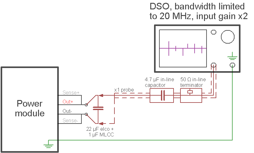
Fig. 21: PARD measurement setup
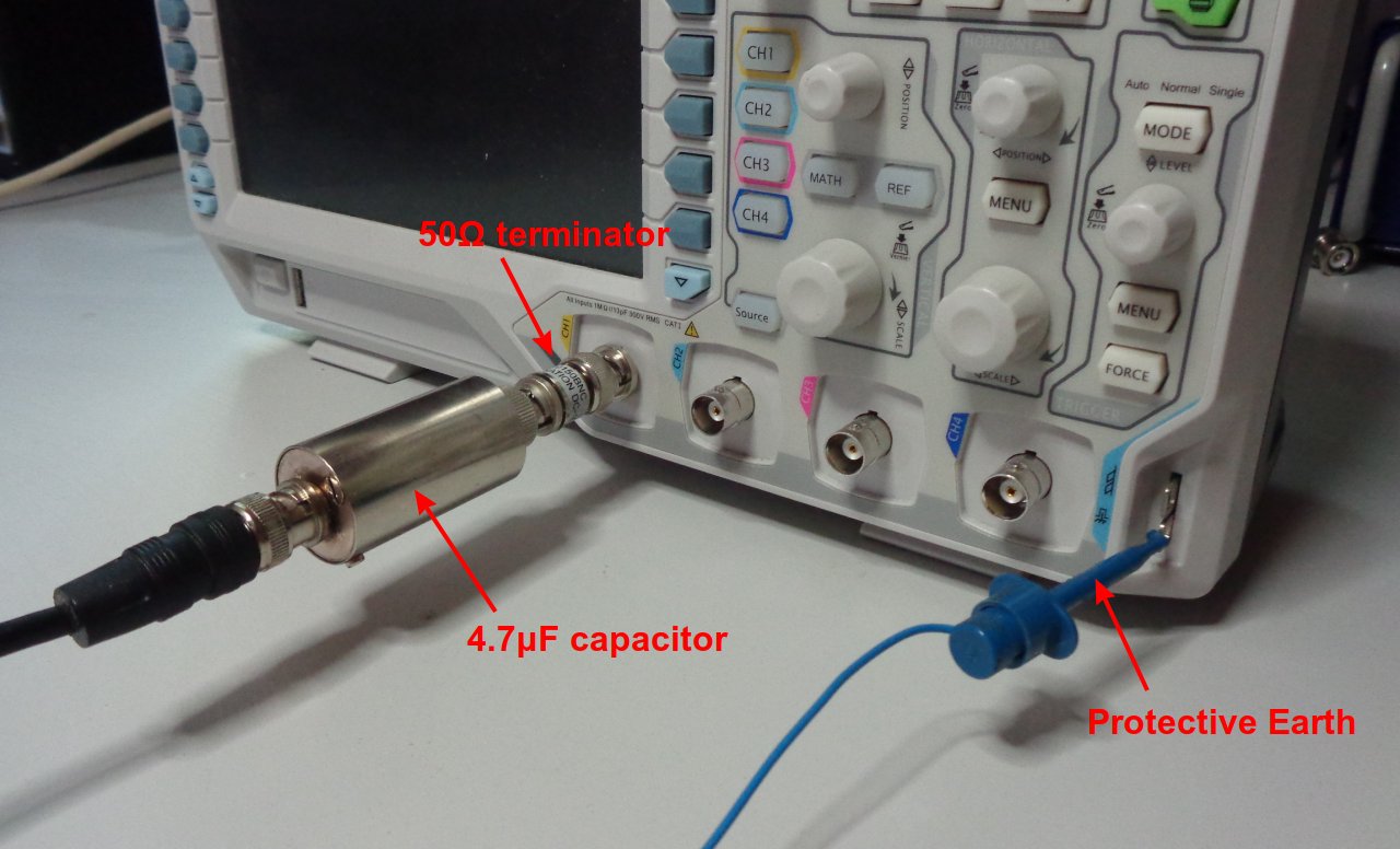
Fig. 22: PARD measurement setup on DSO side
On Fig. 23 is shown DSO own noise when its input is shorted to ground and give us an idea about error that should be taken into account when measuring low level signals such as PARD.
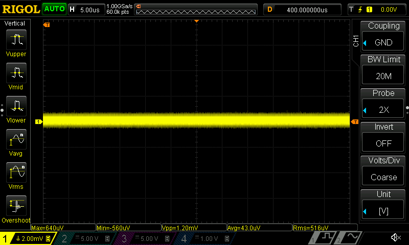
Fig. 23: DSO noise (grounded input)
On the power module side, an additional 22 μF elco + 1 μF MLCC are used where probing is taken place (Fig. 24) because we cannot perform measurement directly on the Cout that is tens of millimeters far away behind the power module front panel. That gives us result shown on Fig. 25 for output current of 1.5 A.
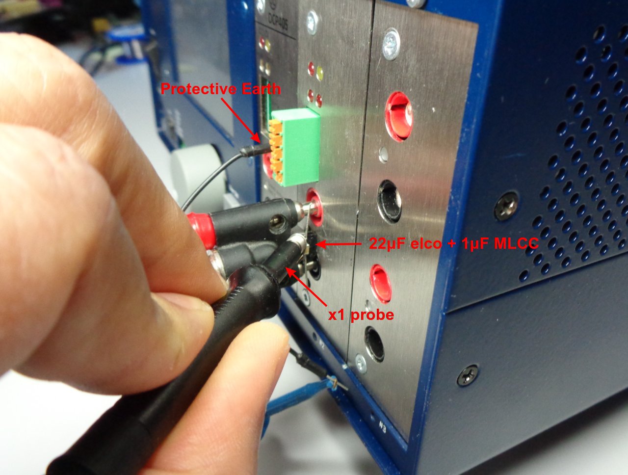
Fig. 24: PARD measurement on power module output with decoupling, Iout = 1.5 A
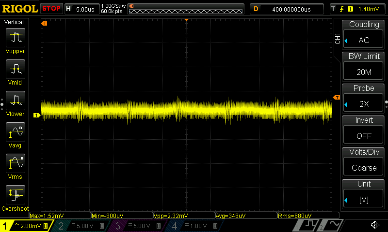
Fig. 25: Output ripple and noise, Iout = 1.5 A
As an example of how setup of such measurement is sensitive, the PARD is also measured on the output of BNC adapter without additional output decoupling on the power terminals (Fig. 26). The results looks much worse but still below 10 mVpp.
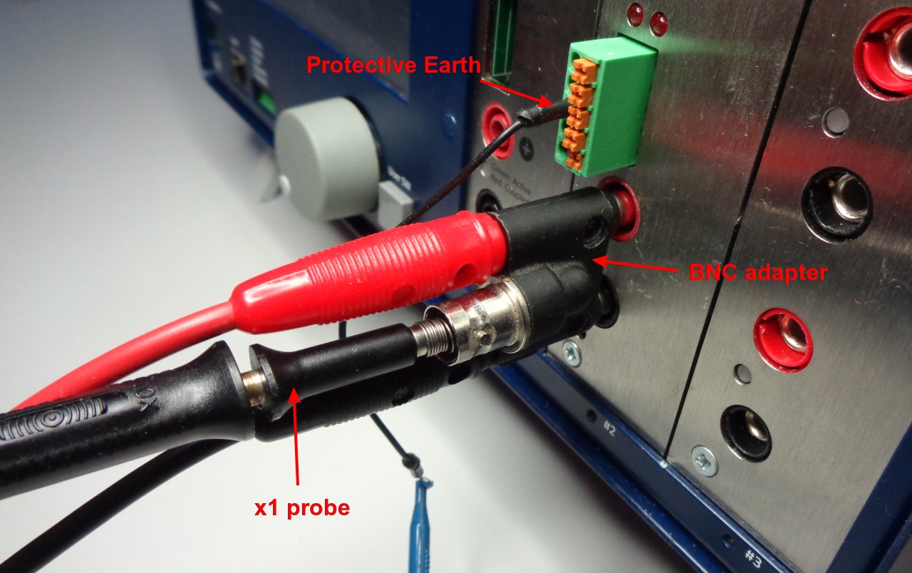
Fig. 26: PARD measurement on BNC adapter, Iout = 1.5 A
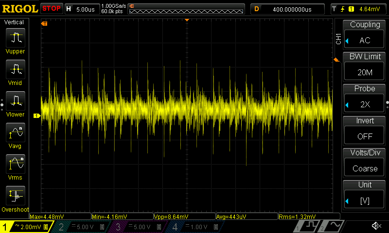
Fig. 27: Output ripple and noise, Iout = 1.5 A
Thermal measurements
Components that are on the power path are exposed to the highest thermal stress due to various loses when DCP405 is delivering the maximum current, i.e. 5 A. Handheld thermal camera Seek Reveal Pro RQ-EAAX is used to inspect temperature of few critical components. The DCP405 module under test was inserted in Slot #1 of the BP3C backplane and the cooling fan is running on the highest speed as it is defined by firmware control algorithm in that case.
The pre-regulator’s power inductor temperature can be seen on Fig. 28. Its temperature is about 60 oC, but we can see on the picture that highest captured temperature is 75 oC and it belongs to area around power MOSFET (Q1) and diode (D2).
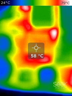
Fig. 28: Pre-regulator’s power inductor, Iout = 5 A
Next area of interest is post-regulator’s “pass” transistors (Q3, Q4) packages that are mounted on the main heatsink. As shown on Fig. 29. their package’s temperature are equal that means they are evenly loaded thanks to balancing resistors.
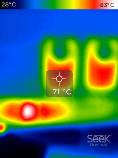
Fig. 29: Post-regulator’s "pass" BJTs, Iout = 5 A
The highest captured temperature on Fig. 29. belongs to balancing resistors R25, R26 as it is shown on Fig. 30.
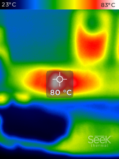
Fig. 30: Post-regulator’s balancing resistors, Iout = 5 A